Nanolithography PowerPoint PPT Presentations
All Time
Recommended
PMMA C6 spun at 4000 RPM onto a Si(100) Substrate: thickness ~ 200 nm ... With feedback off, a relative z offset of 100 nm was added to the z scanner to ...
| PowerPoint PPT presentation | free to download
To go far beyond the Raleigh limit of optical processes, other probes must be applied. By definition a nanostructure is one with nanometer dimensions, but in practice ...
| PowerPoint PPT presentation | free to view
Surface plasmons (SPs) are collective free electron oscillations at a metal ... Surface Plasmon Interference Nanolithography (SPIN) PR. substrate. Z. Liu, et al, Nano. ...
| PowerPoint PPT presentation | free to view
An overview of the global Dip-Pen Nanolithography Technology market, and related technologies and developments. Analyses of global market trends, with historical data from 2018, 2019, and 2020 estimates and projections of CAGRs through 2029. It also includes breakdowns of the overall Dip-Pen Nanolithography Technology market along with various segments, and by geographic region. Analysis of the stakeholder value chain in the Dip-Pen Nanolithography Technology market and comprehensive profiles of leading companies in the industry
| PowerPoint PPT presentation | free to download
Nanolithography And Nanofabrication. ELEC 7950. Special ... cityu.edu.hk/~appkchu/AP4120/5v.pdf. Intel's lithography Roadmap ... Intel's EUV lithography, ...
| PowerPoint PPT presentation | free to view
Nanolithography with diblock copolymers:
| PowerPoint PPT presentation | free to view
Current state of the art photolithography tools use deep ultraviolet light with wave lengths of 248 and 193 nm, which allow minimum feature sizes down to 50 nm.
| PowerPoint PPT presentation | free to view
Sensitivity of the resist (i.e., dosage, C/cm2) Resolution of the D/A board (16 bits ... Positive e-beam resists:-Main-chain scission when exposed to e-beam ...
| PowerPoint PPT presentation | free to view
Usually too high temperatures or other problems with resist in extreme environments ... Heat boat to melt and evaporate metal ... Mechanical gauges, Bourdon. ...
| PowerPoint PPT presentation | free to view
Fabrication of devices using electron-beam lithography. The topics that we will cover in the course are: Overview of lithography ...
| PowerPoint PPT presentation | free to view
B. Multilayer Nanosphere Lithography. Nanosphere lithography was developed by ... nanoparticle array of silver resulting from multilayer nanosphere lithography. ...
| PowerPoint PPT presentation | free to view
Nanolithography Using Bow-tie Nanoantennas Rouin Farshchi EE235 4/18/07 Sundaramurthy et. al., Nano Letters, 6 355-360 (2006) Outline Near-field optics and ...
| PowerPoint PPT presentation | free to view
Oak Ridge National Laboratory. http://homer.hsr.ornl.gov/CBPS ... can write and see Ambient conditions Image from J ... Document presentation ...
| PowerPoint PPT presentation | free to download
An understanding and appreciation of the equipment with which one works is ... Aperture Changer. InLens Detector. 6. How the FESEM Works ...
| PowerPoint PPT presentation | free to view
Block Copolymer Micelle Nanolithography Roman Glass, Martin Moller and Joachim P Spatz University of Heidelberg IOP Nanotechnology (2003) Erika Parra
| PowerPoint PPT presentation | free to view
... Experience at CoE. Nanolithography of Si-Oxide With an Atomic Force Microscope ... The silicon is etched in hydrofluoric acid to remove native oxide layer, and ...
| PowerPoint PPT presentation | free to view
Block Copolymer Micelle Nanolithography Roman Glass, Martin Moller and Joachim P Spatz University of Heidelberg IOP Nanotechnology (2003) Erika Parra
| PowerPoint PPT presentation | free to view
Browse full Report Global Nanolithography Equipment Market 2016-2020 @ http://goo.gl/bw3D9t. The Analysts Forecast Global Nanolithography Equipment market to grow at a CAGR of 0.16%during the period 2016-2020. The report, Global Nanolithography Equipment Market 2016-2020, has been prepared based on an in-depth market analysis with inputs from industry experts. The report covers the market landscape and its growth prospects over the coming years. The report also includes a discussion of the key vendors operating in this market.
AFM Contact Nanolithography Instead, ... Use contact mode for scribing surface AFM Dip-Pen Nanolithography Near field scanning optical microscopy ...
| PowerPoint PPT presentation | free to download
Other fabrication techniques. Photolithography allows one to expose large areas ... More recent fabrication techniques. Dip Pen Nanolithography ...
| PowerPoint PPT presentation | free to view
MNT in Yorkshire & Humberside: Bringing together commercially focused R&D and ... Nanolithography, electron microscopy and magnetics ...
| PowerPoint PPT presentation | free to view
High resolution nanolithography required. Photo taken from: http://news.uns.purdue.edu/UNS/images/chang.quantum.jpeg. Moungi Bawendi (MIT) ...
| PowerPoint PPT presentation | free to view
1 mm. Silica structures. Electrodeposited metal particles coating carbon nanotubes ... was introduced in the 'Advanced Characterization Methods' (Phys 502) class. ...
| PowerPoint PPT presentation | free to view
Silica spheres with carboxylates grafted to the surface to attach novel, Gd free MRI contrast agents (Prof. Stoll). Array of carbon nanotube quantum dots, ...
| PowerPoint PPT presentation | free to download
The Penn State MRSEC hosted the first workshop in 'National Partnership for ... As social scientist observers recorded and analyzed the discussions, these ...
| PowerPoint PPT presentation | free to view
Introduction to Atomic Force Microscopy
| PowerPoint PPT presentation | free to download
... electrochemical cross-linking strategy while patterning, robust and conducting ... are important parameters that affect the patterning and charging experiments. ...
| PowerPoint PPT presentation | free to download
The fabrication of nanoscale features is becoming more ... Fabricate a simple electronic device such as a diode. Fabricate a simple Spintronics device ...
| PowerPoint PPT presentation | free to view
Nanonics produces AFM/SPM systems with unique design for overcoming limitations of standard SPM system. Nanonics offers unique capabilities for integrated microscope of combining SPM with optical microscopy, analytical devices (e.g. Raman) and multiprobe operation.
| PowerPoint PPT presentation | free to download
Nanofabrication of Multicomponent Devices Based on Local Polarization, Photoreaction and Self-assembly Dawn A. Bonnell, A. T. Johnson, W. Degrado, The University of ...
| PowerPoint PPT presentation | free to download
Hemolysin Channel. 2. July 2002. 110nm. 200nm. Issues: ... Relevance. Invest in high-quality, Naval-unique, and Naval-relevant science ...
| PowerPoint PPT presentation | free to view
Title: The California Institute for Telecommunications and Information Technology Author: Jerry Sheehan Last modified by: abennion Created Date: 3/10/1999 2:54:10 PM
| PowerPoint PPT presentation | free to download
... 138.63 1.00 2079441541.68 1.00 10397207.71 1.00 693147180.56 1.00 2180222.32 0.30 1.04e-04 9.90e-05 38508.18 4.62e-03 24067.61 14440.57 231049060.19 1.39e+15 ...
| PowerPoint PPT presentation | free to view
CNT tip is robust, offers amazing resolution. 2 nm thick Au on Mica. MWNT Scanning Probe ... DNA. PROTEIN. High Resolution Imaging of. Biological Materials ...
| PowerPoint PPT presentation | free to view
... interdigiated fingers are actuated by applying a voltage ... z-motion is achieved by electrostatically actuating the cantilever on which the AFM is attached. ...
| PowerPoint PPT presentation | free to view
SPIE Digital Library SPIE Digital Library-SPIE SPIE ( The International Society for Optical Engineering ...
| PowerPoint PPT presentation | free to download
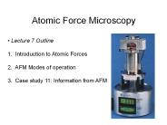
Atomic Force Microscopy Lecture 7 Outline 1. Introduction to Atomic Forces 2. AFM Modes of operation 3. Case study 11: Information from AFM
| PowerPoint PPT presentation | free to download
These challenges and differences of opinion regarding commercial applications are reflected in the widely diverging estimates for the U.S. and global nanotechnology markets.
| PowerPoint PPT presentation | free to download
Saint-Petersburg State Polytechnic University. Center for Advanced Studies ... 'Super-resolution Lithography' Cooperation - NMP. 8. Belgium, UK, ..., Russia ' ...
| PowerPoint PPT presentation | free to download
Faculty Associates: Dimitri Antoniadis (MIT), Yet-Ming Chiang (MIT), W.K. Chim ... Smith (MIT), Francesco Stellacci (MIT), John Thong (NUS), C.C. Wong (NTU), S.F. ...
| PowerPoint PPT presentation | free to view
The Global Printed and Flexible Sensors Market Research Report Forecast 2017-2022 is a valuable source of insightful data for business strategists
| PowerPoint PPT presentation | free to download
... 40 mm biotin spots fabricated on PFP- activated polymer-COOH surfaces via microcontact printing (Chilkoti, 2001) 300 nm spot size IgG nanoarray generated by ...
| PowerPoint PPT presentation | free to download
Developments at the Nano/Bio Interface Point to Scientific Opportunities Functional Molecules and Hybrid Nanostructures Single Molecule Motion and Complexity
| PowerPoint PPT presentation | free to download
'The ability to fabricate, by directed or self-assembly methods, functional ... Examples: Making lighter Golf, Hockey and Base Ball sticks. Applications ...
| PowerPoint PPT presentation | free to view
... is applied to tip while is passes over sample surface. Oxygen bonds attach to ... Voltage is applied to tip while is passes over surface, exposing the PMMA. ...
| PowerPoint PPT presentation | free to view
Bottom-Up Microfabrication Using DNA Presentation Given By: Ben Burns & Janeczka Oates EE 410/510- Microfabrication and Semiconductor Processes University of Alabama ...
| PowerPoint PPT presentation | free to view
Self-cleaning windows, stain-resistant pants, scratch resistant frames. Nantero ... solar cells as thin as wallpaper. Self-assembling solar cells. Healthcare ...
| PowerPoint PPT presentation | free to view
The semiconductor manufacturing industry is undergoing significant changes to address various challenges such as environmental sustainability, climate change, and the shift towards decentralized societies. In this transformative phase, digital technologies play a pivotal role in achieving industry goals, necessitating advancements in semiconductor speed, capacity, and power consumption. However, manufacturers encounter numerous complexities in manufacturing technologies, longer development times, and yield loss in manufacturing, which pose substantial obstacles to progress.
| PowerPoint PPT presentation | free to download
Quartz Crystal Microbalance (QCM) 7. Ellipsometry. A. Tronin et al. ... Quartz Crystal Microbalance. 8. Applications. Anti-static coating for plastics. Sensors ...
| PowerPoint PPT presentation | free to view
Director, California Institute for Telecommunications and ... High Sheer Vortex Emulsifier. Laminar Flow Hood. Standard Biochemical Tools. Planned Facilities: ...
| PowerPoint PPT presentation | free to download
C mo la ptica y la fot nica est n liderando la innovaci n Presentando la Biblioteca Digital de SPIE Marybeth Manning Business Development Director
| PowerPoint PPT presentation | free to download
ANN NIRT GOALI Nano-Engineering Efficient Optoelectronic Devices NSF Grant ECS 0609416 PIs: S. Nikishin, J. Berg, A. Bernussi, M. Holtz, H. Temkin
| PowerPoint PPT presentation | free to download
Microcontact Printing Yes Yes No No No AFM Mechanical Scribing and Nanoindending Overview Yes Yes No No No c-AFM Oxidation A B APDES Nanografted onto SiO2
| PowerPoint PPT presentation | free to download
Global Nanotechnology Market is expected to reach USD 24.56 billion by 2025, from USD 7.24 billion in 2017 growing at a CAGR of 16.5% during the forecast period of 2018 to 2025
| PowerPoint PPT presentation | free to download
epitaxy, self organized growth. organic synthesis ... MOSFET resistor capacitor. Two states: conducting/non-conducting. eg. multiplication (AND) ...
| PowerPoint PPT presentation | free to download


