Etcher PowerPoint PPT Presentations
All Time
Recommended
Title: MATERIALS IN MODERN COMMUNICATIONS SYSTEMS Subject: Elecronic materials lectures Author: Robert W. Hendricks Last modified by: Dr. Kathleen Meehan
| PowerPoint PPT presentation | free to view
Selective etch transfers IC design image on the photoresist to the ... Good and controllable selectivity. All patterned etches are RIE processes in 8' fabs ...
| PowerPoint PPT presentation | free to view
Energy system, thermodynamics and heat transfer. Automatic ... Hitachi Metal etcher. Z A E Design variety. How can we serve our customers. Turn key projects ...
| PowerPoint PPT presentation | free to view
The manual process is subject to error due to human intervention ... The etcher is free to perform other functions during automated etching ...
| PowerPoint PPT presentation | free to view
In this painting, Whistler paid special homage to Rembrandt by painting himself in a similar pose, ... Largely a monochromatic work with a limited color palette, ...
| PowerPoint PPT presentation | free to view
Portable laser engravers are important in many industries for marking many materials due to their ease of operation and industrial compatibility. There are many types and variations of portable laser engravers. At Heatsign, we can provide you with top machines that can produce quality engraved markings. Below are two portable laser engraving machines you should consider.
| PowerPoint PPT presentation | free to download
Bar Code Specified Surgical Pathology Workflow Joy J Mammen MD; Richard Zarbo MD; Adrian Ormsby MD; J. Mark Tuthill MD Henry Ford Health System
| PowerPoint PPT presentation | free to download
In our genre corner , we offer painting of scenes from everyday life, of ordinary people in work or recreation, depicted in a generally realistic manner. Let you feel people’s different life in the world.
| PowerPoint PPT presentation | free to download
Fabricate aluminum microbeams. Develop testing protocol using AFM. Test microbeams ... Fabricate microbeams using IC processing techniques ...
| PowerPoint PPT presentation | free to view
Etching is done either in 'dry' or 'wet' methods ... Use oxidant to oxidize silicon to form silicon dioxide followed by HF etch of silicon dioxide ...
| PowerPoint PPT presentation | free to view
David Ahn Processing Engineer. Kenneth Tseng Equipment Manager ... Remove resist & clean in Piranha dip, 30 sec rinse, and spin dry ...
| PowerPoint PPT presentation | free to view
ETCHING CONTENTS Introduction Basic Concepts Wet etching Plasma etching Manufacturing Methods Plasma etching conditions and issues Plasma etch methods for various ...
| PowerPoint PPT presentation | free to view
Title: Introduction Author: yongsik Last modified by: Timothy D. Duncan Created Date: 4/10/1998 5:16:05 AM Document presentation format: On-screen Show
| PowerPoint PPT presentation | free to download
... so useful work. Additionally Building up to electrospinning requirement of width for edges to be significant portion, needs 3nm diameter.
| PowerPoint PPT presentation | free to view
Processing Capability in UCLAs Nanoelectronics Research Facility NRF
| PowerPoint PPT presentation | free to view
3rd Annual SFR Workshop, November 8, 2000 8:30 9:00 Research and Educational Objectives / Spanos 9:00 9:50 Plasma, Diffusion / Graves, Lieberman, Cheung ...
| PowerPoint PPT presentation | free to download
According to the latest research report by IMARC Group, The global hospital stretchers market size reached US$ 2.8 Billion in 2022. Looking forward, IMARC Group expects the market to reach US$ 3.8 Billion by 2028, exhibiting a growth rate (CAGR) of 5.2% during 2023-2028. More Info:- https://www.imarcgroup.com/hospital-stretchers-market
| PowerPoint PPT presentation | free to download
2. Reactive ion etching for backside of the substrate. Ar CF4. 3. Sample ... The backside layer thickness dependence can help the estimation of the substrate ...
| PowerPoint PPT presentation | free to view
Photoresist Characterization Spin Speed vs. Thickness Nate Hamm, Steve Kelly, Brian MacFarland, John Yarbrough, Jeff Flint Introduction Photolithography is an ...
| PowerPoint PPT presentation | free to download
Spectroscopic ellipsometer for thin film thicknesses and optical properties ... Post-processing - to finish up your devices. CNST Nanofab tools (cont.) Using ...
| PowerPoint PPT presentation | free to view
A Novel Sensor for Monitoring Plasma Reactor Chamber Walls: Simultaneous Monitoring of Ion Flux and Films Deposited on Chamber Walls: SFR Workshop
| PowerPoint PPT presentation | free to download
Apart from this, the growing popularity of aerogel as an effective substitute for glass wool, on account of its higher insulation value, durability, and lightweight, is also catalyzing the global market. Moreover, the implementation of strict regulations by the government bodies regarding noise pollution standards is acting as another significant growth-inducing factor Ask Analyst for Customization and Explore Full Report with TOC & List of Figure: Visit the following link: https://www.imarcgroup.com/acoustic-insulation-market E-mail: sales@imarcgroup.com Contact: +91-120-415-5099
| PowerPoint PPT presentation | free to download
Art of the Dutch and Spanish Masters
| PowerPoint PPT presentation | free to view
A Comparison of Resist Selectivity
| PowerPoint PPT presentation | free to view
... 3 f ff fff3f3 33 3f333 f3 f 3 f 3 f 3 f f ... 3f f ff fff3ff f f f ff 3f ff ffff fffff3fff3 f3f3 f3ff33f3f ff fff3f3 3 3 3 ...
| PowerPoint PPT presentation | free to view
A Comparison of Resist Selectivity
| PowerPoint PPT presentation | free to view
Paste team logos onto master here. Power performance ... Paste team logos onto master here. Epitaxial field-plate. Grown by MBE on SiC ...
| PowerPoint PPT presentation | free to view
Emco High Voltage DC to DC Converters. BY. John Kmiec. Introduction ... a wide variety of high voltage DC-DC converters ranging from 100V to 30000V and ...
| PowerPoint PPT presentation | free to view
Rembrandt Harmenszoon van Rijn was born on July 15, 1606, in Leiden, the Netherlands. ... in the 1640s and 1650s, but his financial circumstances were not unbearable. ...
| PowerPoint PPT presentation | free to view
Peripheral clamping of the wafer to the chuck ... Use electrostatic clamping of the wafer(ECE) ... Provides a uniform clamping force over the wafer surface ...
| PowerPoint PPT presentation | free to view
Brigham Young University Microfabrication Group. Microfabrication Mentoring Environment ... Brigham Young University Microfabrication Group. MME ...
| PowerPoint PPT presentation | free to view
... photoresist grating structures prevents angularly dispersed ions from striking ... turn should lead to more angularly dispersed ions and hence more severe ...
| PowerPoint PPT presentation | free to view
http://kstar.knfp.net/kpsdpp/KPS_Poster/2002_kps/pdf_file ... 8300A thick DUV photo resist with a hole patterns of 0.19 micron in diameter was ...
| PowerPoint PPT presentation | free to view
In any case, cheats think that it’s alluring to be stolen because of its esteem and the carelessness of the proprietor too. All in all, are there any approaches to guarantee boat security and spare it from getting stolen? Indeed, we should view them in detail.
| PowerPoint PPT presentation | free to download
This technology gives us flexibility to freely adjust the deposited layers ... Compact Arrayed Waveguide Grating Demulti-plexers Based on Amorphous Silicon Nanowires ...
| PowerPoint PPT presentation | free to view
Title: Advancing RIT to Submicron Technology: Design and Fabrication of 0.5 um N-Channel MOS Transistors Author: Mike Last modified by: lffeee Created Date
| PowerPoint PPT presentation | free to view
Estimation of Etch Depth for Blanket Wafers. Estimation for Patterned Wafers ... Pre-etch thickness measured using a Spectral Photometer. Accuracy /- 20 ...
| PowerPoint PPT presentation | free to view
... MS2001 Dump-rinse Spin Dry Inspection Post ICP Deep Silicon Etch Polymer Removal Clean CMOS/Non ... Technology Gene Chip Compound Semiconductor ...
| PowerPoint PPT presentation | free to download
Depending on the photo-resist and its corresponding viscosity, sometimes the ... 1. Merriam-Webster Online Dictionary. www.m-w.com ...
| PowerPoint PPT presentation | free to view
Small Feature Reproducibility A Focus on Semiconductor Technology Education UC-SMART Major Program Award D.B. Graves, T.J. King, and C.J. Spanos
| PowerPoint PPT presentation | free to download
Rolly Guerrero 396. Web Designer, Circuit Specialist. Landon Barayuga 396. Computer Programmer ... Detecting intersections and dead ends (and maneuvering accordingly) ...
| PowerPoint PPT presentation | free to view
Process Control, Modeling and Diagnosis S. Joe Qin Department of Chemical Engineering The University of Texas at Austin Austin, Texas 78712 512-471-4417
| PowerPoint PPT presentation | free to download
Overview of Nanofabrication Material depostion methods Thin films of materials Thickness measurement Lithography Pattern transformation on to planar suface
| PowerPoint PPT presentation | free to view
The Birck Nanotechnology Center
| PowerPoint PPT presentation | free to view
The more complex the system, the more service and higher user costs. Industry Fab. ... Photo Lithography. UV, deep UV. Projection or contact. Micro contact printing ...
| PowerPoint PPT presentation | free to view
terms of net etch rate and in resulting etch profile. ... Avant!'s TAURUS-TOPOGRAPHY. simulation using their dry etch. model with simultaneous polymer ...
| PowerPoint PPT presentation | free to view
... cathode, shuttle with mechanical clamping to maintain shuttle temperature below ... Clamping. Loading tool. Cathode. Shuttle. Cooling. Loading tool. Cathode ...
| PowerPoint PPT presentation | free to view
Professor James Yardley Director NSEC 4-3839 ... for Chromium (chrome logs supplied for Thermal Evaporators as are. Tungsten boats) ...
| PowerPoint PPT presentation | free to view
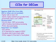
Lick Guider (2x) (1 with 2-stage amp) SNAP 9 mm. Pixel spectrograph. CCD 2226 x 868 ... Packaging going on at Lick, Yale Arizona. 6/25/09 ...
| PowerPoint PPT presentation | free to download
Title: MAPLD 2001 Figures for Talk B4 Author: McCollumJ Last modified by: Richard B. Katz Created Date: 8/29/2001 12:23:54 AM Document presentation format
| PowerPoint PPT presentation | free to view
Texas Medical Center. Houston, TX. Application Deadline: Feb. 15 ... Texas Medical Center. Houston, TX. Application Deadline: Feb. 15. Program Features ...
| PowerPoint PPT presentation | free to view
Title: No Slide Title Author: Rod Boswell Last modified by: Rod Created Date: 8/27/2002 5:38:48 AM Document presentation format: On-screen Show (4:3)
| PowerPoint PPT presentation | free to view
Semiconductor Polymer Integrated Fabrication Facility
| PowerPoint PPT presentation | free to download
analysis. Corrective. actions. Inspection. Validation. Goal ... information as it arrives by incorporating it into the new product or process under development ...
| PowerPoint PPT presentation | free to download
XTEST2 A first Belle Pixel Readout Prototype Gary S. Varner University of Hawai,i Overview A number of options for readout of a pixel sensor for use in a B-Factory ...
| PowerPoint PPT presentation | free to download


