
Wafer Laser Marking PowerPoint PPT Presentations
All Time
Recommended

If you're in the business of making silicon wafers, you've probably heard about the importance of semiconductor wafer inspection.
| PowerPoint PPT presentation | free to download

WLSC (Worldwide Laser Service Corporation) is one of the top companies offers Fiber Laser Marking services in USA. Get finest Fiber Laser Marking service for your business products. Visit the website to know more. https://wlsc.com/2018/01/fiber-laser-marking/
| PowerPoint PPT presentation | free to download

According to the latest research report by IMARC Group, The global fiber laser market size reached US$ 2.5 Billion in 2022. Looking forward, IMARC Group expects the market to reach US$ 4.3 Billion by 2028, exhibiting a growth rate (CAGR) of 9.2% during 2023-2028. More Info:- https://www.imarcgroup.com/fiber-laser-market
| PowerPoint PPT presentation | free to download

Looking forward, the fiber laser market value is projected to reach a strong growth during the forecast period (2022-2027). More info:- https://www.imarcgroup.com/fiber-laser-market
| PowerPoint PPT presentation | free to download

????????? YAG-??????. Steered beam Nd:YAG laser marking systems. Videojet LN100A ... Page 31. ??????? ?????????? YAG-??????? Application examples Nd:YAG ...
| PowerPoint PPT presentation | free to view

Review of many of the major applications of lasers (and a few daft ones) ... components prior to welding and PCB's and component leads prior to soldering. ...
| PowerPoint PPT presentation | free to view

In a process known as silicon Wafer Inspection and cleaning, particles on the surface must be removed from the surface. The process of silicon Wafer Polishing starts with removing any defects. If new material is used to produce a silicon wafer, it can create roughness on the surface. This is an important step in the process before a wafer reaches the fabrication facility (fab).
| PowerPoint PPT presentation | free to view

The gallium nitride semiconductor device market is expected to reach USD 22.47 Billion by 2023 at a CAGR of 4.6% during the forecast period. https://www.marketsandmarkets.com/Market-Reports/gallium-nitride-gan-semiconductor-materials-devices-market-698.html
| PowerPoint PPT presentation | free to download

In this article we have discussed four different types of laser engraving machines, its uses, benefits, and ways you can use it in your day to day business.
| PowerPoint PPT presentation | free to download

Bulk Al (cheap) CVD SiC ($550 for 3-cm disk, l/50, 2 ) ... SEM photos of damaged Al. 1 mm. 20 mm. The UCSD laser lab is used to test GIMMs ...
| PowerPoint PPT presentation | free to view
AIM Industrial Advisory Committee Meeting 7 April 2004. Course Goal: Multidisciplinary learning ... Laser vibrometer. Signal analyzer. Vdisplacement. Vstrain ...
| PowerPoint PPT presentation | free to download

Laser Re-Crystallization uses a laser to scan polycrystalline silicon on the ... it and allowing it to re-crystallize forming a single-crystal material matched ...
| PowerPoint PPT presentation | free to view
Semiconductors Presented by Aman Bansi Mark Thomlinson Barnard Choi Agenda Industry overview Intel AMD Applied Materials A Brief History Pre-1950 s - Vacuum tubes ...
| PowerPoint PPT presentation | free to download
Micro to Nano Technologies By: Brent Hare Lenox laser March 30, 2004 Micro to Nano Technologies Micro - Prefix meaning one millionth, 1/1,000,000 Nano Prefix ...
| PowerPoint PPT presentation | free to download

During PEB, photo-acid diffusion causes amplification in a catalytic reaction ... Scanning Projection System. Synchronized mask and wafer movement. Slit. Lens ...
| PowerPoint PPT presentation | free to view

RETROREFLECTOR ARRAYS FOR SPACE SHUTTLE AND SPACE STATION DOCKING, ESA AND NASA ... LRR-LASER SATELITE TRACKING. LANDWARRIOR. SBL-LIGHT WEIGHT MIRRORS ...
| PowerPoint PPT presentation | free to view

Integrated Smart Nanosensors for Space Biotechnology Applications Toshikazu Nishida Mark E. Law University of Florida NASA Research Briefing September 25, 2002
| PowerPoint PPT presentation | free to view

Remove specific portion of the layer on wafer surface (oxide, dielectrics, metal) ... 0.35 mm), ECR (electron cyclotron resonance), ICP(inductively coupled plasma) ...
| PowerPoint PPT presentation | free to view

laser beam is reflected off a spot on the cantilever to photodiode that detects the ... photodiode then controls force on cantilever so that it remains constant ' ...
| PowerPoint PPT presentation | free to view

Beginners, even under close supervision by a master of the art, will invariably ... The following picture shows a photography of a Si wafer that was preferentially ...
| PowerPoint PPT presentation | free to view

A leading supplier of silicon wafers, wafer processing, semiconductor Equipment, Ceramic Packages, Wafer fabrication, chip carriers and operation Management

Non-contact High resolution. Custom probe sizes High frequency response. Accurate Reliable ... High-resolution LCD display. Adjustable stage for precise leveling ...
| PowerPoint PPT presentation | free to download

Universidade Federal do Rio Grande do Sul Engenharia El trica Circuitos Eletr nicos Integrados ENG04061 Testes de Circuitos Eletr nicos Integrados
| PowerPoint PPT presentation | free to view

Innovative method for sapphire substrate dicing: Intrascribe ... Sapphire Scribing System production and supply. MULTITECH Ltd. 190103, Russia, Saint-Petersburg, ...
| PowerPoint PPT presentation | free to view

Lithography Lithography in the MEMS context is typically the transfer of a pattern to a photosensitive material by selective exposure to a radiation source such as light.
| PowerPoint PPT presentation | free to download

2002 . 8 . 16 MAI Lab MAI Lab Seminar Film Deposition Deposition Application STI (Shallow Trench Isolation) Junction Isolation ...
| PowerPoint PPT presentation | free to view
Exploring Light: The Optics of Diffraction. McDonald Observatory. The University of Texas at Austin ... Some spectrometers at McDonald Observatory ...
| PowerPoint PPT presentation | free to download

Ming-Cheng Sheng ASEKH-IT April 9, 2003 Agenda IT Requirement for Assembly & Testing House Business Model ASEKH-Test IT ...
| PowerPoint PPT presentation | free to download

Title: PowerPoint Presentation Last modified by: Joneja Created Date: 1/1/1601 12:00:00 AM Document presentation format: On-screen Show Other titles
| PowerPoint PPT presentation | free to view


Task 2 Optical Interconnects
| PowerPoint PPT presentation | free to view

* * * * * * * * AGENDA Introduction to dual frequency capacitively coupled plasma ... Institute for Plasma Science & Engr. Inductively coupled plasma with multi ...
| PowerPoint PPT presentation | free to download

A Company Overview
| PowerPoint PPT presentation | free to view

Brigham Young University Microfabrication Group. Microfabrication Mentoring Environment ... Brigham Young University Microfabrication Group. MME ...
| PowerPoint PPT presentation | free to view

Title: Piezoresistive Cantilevers for the Characterization of Gold MicroContacts Author: Beth Pruitt Last modified by: Michael Kelly Created Date
| PowerPoint PPT presentation | free to download

UCOLick Laboratory for Adaptive Optics Developing Adaptive Optics for the Next Generation of Astrono
| PowerPoint PPT presentation | free to view

Nanotechnology using Electron Beam Lithography, Center for Quantum Devices ... Two-dimensional photonic crystal waveguide obtained by e-beam direct writing of ...
| PowerPoint PPT presentation | free to view

UCOLick Laboratory for Adaptive Optics Developing Adaptive Optics for the Next Generation of Astrono
| PowerPoint PPT presentation | free to view

In: Current Issues in Heteroepitaxial Growth - Stress Relaxation and Self-Assembly. ... Stress free, alignment tolerant, hybrid integration scheme ...
| PowerPoint PPT presentation | free to view

FLCC Feature-level Compensation & Control Overview April 5, 2006 A UC Discovery Project
| PowerPoint PPT presentation | free to download

Testing and burn-in cost mitigated with more I/O and WL approach. Chip-to ... Approach: Develop smart algorithms using sensor fusion and possibility theory ...
| PowerPoint PPT presentation | free to view
Agilent 7500 Series ICP-MS An Introduction Presented By: Ferdi Ferdian Kusnadhi What is ICP-MS? ICP - Inductively Coupled Plasma high temperature ion source ...
| PowerPoint PPT presentation | free to download

Hot test is usually most critical since speed is key differentiator (devices ... This will reduce devices which fail during burnin or at class (speed) test. ...
| PowerPoint PPT presentation | free to view

Overview of Nanofabrication Material depostion methods Thin films of materials Thickness measurement Lithography Pattern transformation on to planar suface
| PowerPoint PPT presentation | free to view
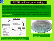
MEMS and sensors technology Recent development of MEMS and sensors technology is essentially based on micromachinig. This technology consists of specific design and ...
| PowerPoint PPT presentation | free to download

332:578 Deep Submicron VLSI Design Lecture 4 CMOS Deep Submicron Fabrication Technology
| PowerPoint PPT presentation | free to view

S. E. Thompson EEL 6935. Today's Subject. Continue on some basics on single-wall ... (a) armchair (5, 5), (b) zigzag (9, 0), and (c) zigzag (10, 0) carbon nanotubes. ...
| PowerPoint PPT presentation | free to view

What a role does the microelectronics play in life of the modern society? ... Short gate MOSFET structure. Electron microscope picture of the MOSFET structure ...
| PowerPoint PPT presentation | free to view

Optical and RF technologies for on-chip and off-chip ... Trimming and tuning may be necessary. Interconnect Focus Center. e. e. e. e. GaAs ...
| PowerPoint PPT presentation | free to view

Plasma etching is a dry etching method. ... ( John L. Vossen, Aerner Kern, Thin Film Processes II, Academic Press Inc.) Reactive gas etching ...
| PowerPoint PPT presentation | free to view

PDF417 symbology inside of an automobile door frame ... Matrix symbologies offer higher data densities ... a member of the RSS (Reduced Space Symbology) family ...
| PowerPoint PPT presentation | free to view

1980s: O/S (including a database) and apps. VAX/VMS Architecture (and architects) ... apps are bound to a configuration & VendorIX! network is NOT the computer ...
| PowerPoint PPT presentation | free to download

JEOL JBX-5000LS. Jan H. Kuypers. Esashi Ono Tanaka ... would leave streaks in our resist pattern, so ... streak to the left. beam blanker. conjugate blanking ...
| PowerPoint PPT presentation | free to view

Identify the major hardware ... Comfortable ergonomics. Uncomfortable ergonomics (small keyboard, often with inconvenient placement of function keys) ...
| PowerPoint PPT presentation | free to view
Computer Hardware How to Choose a Multimedia Computer Plymouth State University
| PowerPoint PPT presentation | free to download