
Vtn PowerPoint PPT Presentations
All Time
Recommended

Non-human primate challenge studies. GLP-compliant regulatory studies. Clinical Trials ... Experiments in rodents and primates. Human trials. Safety, immunogenicity ...
| PowerPoint PPT presentation | free to view

Data Networks: FAS, SAN, NAS. Data Recovery. Tape Backup ... Data Recovery Tape Backup. Intrusion Prevention/Detection. Anti-Virus, Anti-Spam, Firewalls ...
| PowerPoint PPT presentation | free to view

Reflect p device characteristic about x-axis. Take absolute value of p device characteristic ... With Idsp = - Idsn, then. Vout = (Vin Vtn) - (Vin Vtn)2 ...
| PowerPoint PPT presentation | free to view

Amp. Volt. VDD. isc(t) 0. Vi(t) Vo(t) VDD - VTp. VTn. tB. tE. Iscmaxf ... Other forms of scaling are referred to as constant-voltage and quasi-constant-voltage. ...
| PowerPoint PPT presentation | free to download

Background Original CJIN Voice Trunking Network (VTN) Recommended in the 1995 CJIN Legislative Study by Price Waterhouse Re-Validated in CJIN re-fresh study in 2002 ...
| PowerPoint PPT presentation | free to view

nMOS pass transistors pull no higher than VDD-Vtn. Called a degraded '1' ... If bp / bn 1, switching point will move from VDD/2. Called skewed gate ...
| PowerPoint PPT presentation | free to view

Introduce global var. to TYP-Vth. A0. TYP-Vth. 11 /27. Vtn. Concept of 'Vth Curves' 4. ... SNML is a function of. AC2, DR1, DR2 and LD1. AC1. DR1. DR2. AC2. LD1 ...
| PowerPoint PPT presentation | free to view

What really happens if VGS VTN? In digital design, IDS = 0. ... Note: This is not really true due to recombination, but its close! ECE 584, Summer 2002 ...
| PowerPoint PPT presentation | free to view

Axioms - basic properties assumed to be true (A1) X= if X1 (A1' ... AMIS 1.5 m: k'p=-11.4 A/V2 Vtp=-1.02V. k'n= 34.2 A/V2 Vtn=0.61V. Rn. Rp. VDD=5V. VDD=3.3V ...
| PowerPoint PPT presentation | free to view

CEG3470 REVISION LECTURE (Some s from Introduction to CMOS VLSI Design Lecture 4: DC & Transient Response) David Harris Harvey Mudd College Spring 2004
| PowerPoint PPT presentation | free to download

Figure 4.2 - MOS capacitor operating in (a) accumulation (b) depletion (c) inversion. Figure 4.3 - (a) NMOS transistor structure (b) cross section
| PowerPoint PPT presentation | free to view

Requires solving differential equations. Input is usually considered to be a step or ramp ... Solving differential equations by hand is too hard ...
| PowerPoint PPT presentation | free to download
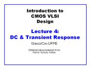
Introduction to CMOS VLSI Design Lecture 4: DC & Transient Response Greco/Cin-UFPE (Material taken/adapted from Harris lecture notes) ...
| PowerPoint PPT presentation | free to download

DC & Transient Response. David Harris. Harvey Mudd College. Spring 2004 ... DC Response. Logic Levels and Noise Margins. Transient Response. Delay Estimation ...
| PowerPoint PPT presentation | free to download

... (NML): tolerable voltage range for which we interpret the inverter output as a logic 0 NML = VIL - VOL Switch Representation Switching Dynamics Input high: ...
| PowerPoint PPT presentation | free to download

Recall Lecture 17 MOSFET DC Analysis Using GS (SG) Loop to calculate VGS Remember that there is NO gate current! Assume in saturation Calculate ID using saturation ...
| PowerPoint PPT presentation | free to view

Title: MOSFET Small Signal Equivalent Ckt Subject: saved backup 4 Author: hutchens Last modified by: Windows User Created Date: 1/9/1998 7:08:36 PM
| PowerPoint PPT presentation | free to view

Field-Effect Transistors Microelectronic Circuit Design Richard C. Jaeger Travis N. Blalock Microelectronic Circuit Design, 4E McGraw-Hill Chap 4-* ...
| PowerPoint PPT presentation | free to view

Title: Author: fap Last modified by: qw Created Date: 11/24/2001 9:02:01 AM Document presentation format:
| PowerPoint PPT presentation | free to view

Chapter 5 Field-Effect Transistors
| PowerPoint PPT presentation | free to view

Microelectronics Circuit Analysis and Design Donald A. Neamen Chapter 3 The Field Effect Transistor Neamen Microelectronics, 4e Chapter 3-1 McGraw-Hill
| PowerPoint PPT presentation | free to view

Lecture 21 OUTLINE The MOSFET (cont d) P-channel MOSFET CMOS inverter analysis Sub-threshold current Small signal model Reading: Pierret 17.3; Hu 6.7, 7.2
| PowerPoint PPT presentation | free to view
Title: Slide Title Author: Dhamin Al-Khalili Description: Some of the material has been copied from Rabaey/Prentice Hall Last modified by: Concordia university
| PowerPoint PPT presentation | free to download

Mask ROM, PROM, EPROM, and EEPROM ... EPROM, EEPROM, FPGA, Flash, FRAM. 6-5. Laboratory of Reliable Computing. Memory Architecture ...
| PowerPoint PPT presentation | free to view
Body effect parameter Channel length modulation parameter PMOSFET I-V ... Problem with the Square Law Theory Ignores variation in depletion width with ...
| PowerPoint PPT presentation | free to download

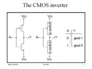
Arial Book Antiqua Monotype Sorts Times New Roman iab97 Microsoft Equation 3.0 CMOS INVERTER DIGITAL GATES Fundamental Parameters The Ideal Gate VTC of Real ...
| PowerPoint PPT presentation | free to view

Clocked CMOS. 5-4. Laboratory of Reliable Computing. C2MOS: AND and OR function. 5-5 ... Estimate the Vo decreasing rate with initial condition of Vo=4V and iL ...
| PowerPoint PPT presentation | free to view

NMOS Device Physics. PMOS Device Physics. CMOS Inverter. MOSFET ... Equation: ... Appropriate I-V equations found by: 1) reversing the direction of ID ...
| PowerPoint PPT presentation | free to download

Velocity saturation limits IDSsat in modern MOSFETS. Simple model: ... projectile-like motion ('ballistic transport') The average velocity of carriers exceeds vsat ...
| PowerPoint PPT presentation | free to view
Power Dissipation in CMOS Static Power Consumption Static Power Dissipation Subthreshold Current Subthreshold Current Analysis of CMOS circuit power dissipation The ...
| PowerPoint PPT presentation | free to download
Universidade Federal de Santa Catarina Centro Tecnol gico Computer Science & Electrical Engineering Digital Integrated Circuits INE 5442 / EEL 7312
| PowerPoint PPT presentation | free to download

Concep o de Circuitos Integrados Modelos doTransistor MOS Inform tica UFRGS P fonte dreno grade canal N Transistor MOS xido de gate VGS + - substrato P xido ...
| PowerPoint PPT presentation | free to view

Neamen, Electronic Circuits Analysis And Design, 2nd ed. Chapter 16. 4-3 ... Laboratory of Reliable Computing. Current-Voltage of NMOS and PMOS. 4-6 ...
| PowerPoint PPT presentation | free to view

CMOS Differential Amplifier Lab 7 2weeks Diff Amp SPICE Models: NMOS LEVEL=2 +VTO=-0.7 KP=5000E-6 LAMBDA=0.02 GAMMA=0.45 +TOX=90E-9 NSUB=3.7E15 PMOS LEVEL=2 +VTO=0.7 ...
| PowerPoint PPT presentation | free to download

Miller 1953. doubled F0 and found vowel category shift for most American English vowels ... Peterson, G. E. & Barney, H. L. (1952) Control methods used in the ...
| PowerPoint PPT presentation | free to download

... Project. Expectation. To introduce you to basic research ideas ... Involves reading research paper. Extraction of relevant parameters. Simulation of circuits ...
| PowerPoint PPT presentation | free to view
Chapter 6 Dynamic CMOS Circuits Boonchuay Supmonchai Integrated Design Application Research (IDAR) Laboratory August 15, 2004; Revised - July 4, 2005
| PowerPoint PPT presentation | free to download
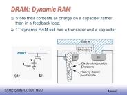
Store their contents as charge on a capacitor rather than in a feedback loop. ... 3. read disturbs the cell content at x, so the cell must be rewritten after each ...
| PowerPoint PPT presentation | free to download

ELEC 5970-001/6970-001(Fall 2005) Special Topics in Electrical Engineering Low-Power Design of Electronic Circuits Power Consumption in a CMOS Circuit
| PowerPoint PPT presentation | free to download

Very low voltage 16-bit counter in high leakage static CMOS technology COLIN STEVENS LOW POWER ELECTRONICS ELEC6270 INSTRUCTOR-VISHWANI D. AGRAWAL
| PowerPoint PPT presentation | free to download

Nortel Networks, Canada. IP-Networking/Mediacom Workshop, 24 -27 April 2001. 2. Outline ... Decoupling of services from Access & Transport technologies allows: ...
| PowerPoint PPT presentation | free to download

Title: Slide 1 Author: NGAN HANG MAU Last modified by: User Created Date: 8/16/2006 12:00:00 AM Document presentation format: On-screen Show Other titles
| PowerPoint PPT presentation | free to view

Rabaey Amirkabir University of Technology
| PowerPoint PPT presentation | free to download
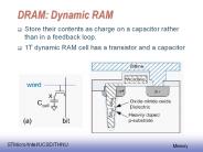
DRAM: Dynamic RAM Store their contents as charge on a capacitor rather than in a feedback loop. 1T dynamic RAM cell has a transistor and a capacitor
| PowerPoint PPT presentation | free to download

Internet izvor geografskog znanja? Diplomski rad Silvia Pavi
| PowerPoint PPT presentation | free to download

Norfolk (OFK) Omaha (OMA) Methodology (Continued) ... OFK Start Times... Avg Start Time = 20:14Z (14:14LST / 15:14 LDT) Avg Event Length ~ 2.7 hours ...
| PowerPoint PPT presentation | free to download

Switching of Output from 1 to 0 begins when Vin exceeds Vt of pull down device ... Pull-Up to Pull-Down Ratio for an nMOS inverter driven. through 1 or more ...
| PowerPoint PPT presentation | free to view

Lecture 42: Review of active MOSFET circuits Prof. J. S. Smith Final Exam Covers the course from the beginning Date/Time: SATURDAY, MAY 15, 2004 8-11A Location ...
| PowerPoint PPT presentation | free to view

REAPDOR sequence for measuring dipolar couplings between I 1 ... Investigating reaction products. Chemical shift information. ppm. 13C-CP-MAS. Tolane sample ...
| PowerPoint PPT presentation | free to view

ELEC 5970-001/6970-001(Fall 2005) Special Topics in Electrical Engineering ... Charge recovery and adiabatic switching circuits. Simulation-based power estimation tool ...
| PowerPoint PPT presentation | free to download
The dynamic power dissipation is a function of: Frequency. Capacitive loading. Voltage swing ... To reduce dynamic power dissipation. Reduce: CL. Reduce: f ...
| PowerPoint PPT presentation | free to download
Aucun titre de diapositive - jonathan.amiach.free.fr ... introduction
| PowerPoint PPT presentation | free to download
pMOS fights nMOS. 9: Circuit Families. Slide 6. CMOS VLSI Design. Pseudo-nMOS Gates ... evaluation transistor to prevent fight. 9: Circuit Families. Slide 14 ...
| PowerPoint PPT presentation | free to download

Jaeger/Blalock. 7/1/03. Microelectronic Circuit Design. McGraw-Hill. Chapter 13 ... Richard C. Jaeger. Travis N. Blalock. Chap13 - 1. Jaeger/Blalock. 7/1/03 ...
| PowerPoint PPT presentation | free to view

Title: RS_Overview Author: Nehru Last modified by: carmen Created Date: 6/2/1995 10:09:48 PM Document presentation format: Presentaci n en pantalla
| PowerPoint PPT presentation | free to view

Introduction to CMOS VLSI Design Lecture 3: CMOS Transistor Theory David Harris Harvey Mudd College Spring 2004 Outline Introduction MOS Capacitor nMOS I-V ...
| PowerPoint PPT presentation | free to view