Subproject: MEMSbased nanopatterning - PowerPoint PPT Presentation
1 / 2
Title:
Subproject: MEMSbased nanopatterning
Description:
The subproject MEMS deals with the development of new micro-mechanical tools for ... full wafer scale with 1 micrometer alignment accuracy, on CMOS circuitry. ... – PowerPoint PPT presentation
Number of Views:36
Avg rating:3.0/5.0
Title: Subproject: MEMSbased nanopatterning
1
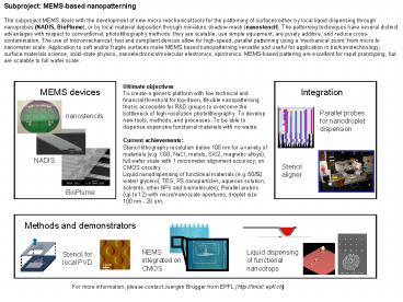
Subproject MEMS-based nanopatterning The
subproject MEMS deals with the development of new
micro-mechanical tools for the patterning of
surfaces either by local liquid dispensing
through nanoprobes (NADIS, BioPlume), or by local
material deposition through miniature shadow-mask
(nanostencil). The patterning techniques have
several distinct advantages with respect to
conventional, photolithography methods they are
scalable, use simple equipment, are purely
additive, and reduce cross-contamination. The use
of micromechanical, fast and compliant devices
allow for high-speed, parallel patterning using a
mechanical zoom from micro to nanometer scale.
Application to soft and/or fragile surfaces make
MEMS based nanopatterning versatile and useful
for application in bio/nanotechnology, surface
materials science, solid-state physics,
nanoelectronics/molecular electronics,
spintronics. MEMS-based pattering are excellent
for rapid prototyping, but are scalable to full
wafer scale.
Ultimate objectives To create a generic platform
with low technical and financial threshold for
top-down, flexible nanopatterning that is
accessible for RD groups to overcome the
bottleneck of high resolution photolithography.
To develop new tools, methods, and processes. To
be able to dispense expensive functional
materials with no waste. Current
achievements Stencil lithography resolution
below 100 nm for a variety of materials (e.g.
C60, NaCl, metals, SiO2, magnetic alloys), full
wafer scale with 1 micrometer alignment accuracy,
on CMOS circuitry. Liquid nanodispensing of
functional materials (e.g. 50/50 water/ glycerol,
TEG, PS nanoparticles, aqueous solution,
solvents, other NPs and biomolecules) Parallel
probes (up to 12) with micro/nanoscale apertures,
droplet size 100 nm - 20 um
MEMS devices
Integration
Parallel probes for nanodroplet dispension
nanostencils
NADIS
Stencil aligner
BioPlume
Methods and demonstrators
NEMS integrated on CMOS
Liquid dispensing of functional nanodrops
Stencil for local PVD
For more information, please contact Juergen
Brugger from EPFL (http//lmis1.epfl.ch)
2
(No Transcript)


