Wafer Stages PowerPoint PPT Presentations
All Time
Recommended
Wafer cassette mapping and wafer front end are going to help you make the most out of your business. To locate the provider rendering a wide variety of good quality wafer cassettes mapping services, you need to make sure to look out for some real pros. Let's check out the PPT for more info.
| PowerPoint PPT presentation | free to download
Are you looking for wafer robot repair solutions? Kensington Laboratories offers certified products of precision handling robots to stage repair programs that can help smooth out industry operations and offer you value for money.
| PowerPoint PPT presentation | free to download
In simple words, Silicon wafer reclaim is the method of restoring a used wafer to its original state at a lower cost. This is unquestionably a more cost-effective choice than purchasing fresh wafers.
| PowerPoint PPT presentation | free to download
Wafer pre aligners are a very vital component in the manufacturing of wafers. The positioning precision highly affects the exposure accuracy of the wafer and efficiency of the work in the whole manufacturing system. Just read out the PPT you will come to know reasons and features that why wafer pre aligners is an important part of the wafer transmitting system.
| PowerPoint PPT presentation | free to download
The semiconductor industry is improving daily, either for the production equipment manufacturers or the end-users. In fact, the transistors in the integrated circuit are getting increased along with the performance.
| PowerPoint PPT presentation | free to download
Kensington’s precision linear stages position substrates, silicon wafers and photonic devices, quickly with precision and repeatably.
| PowerPoint PPT presentation | free to download
Kensington is a leading supplier of wafer handling robots, precision motion control, linear stages, rotary stages, and integrated stages designed to meet the most demanding requirements. We provide technical services all over the US. Read this ppt to get more info.
| PowerPoint PPT presentation | free to download
Kensington builds wafer handling robots and precision motion control stages then supports them with exceptional service for a lifetime of productivity.
| PowerPoint PPT presentation | free to download
Kensington Laboratories is a semiconductor equipment manufacturing and service company. The leading supplier is committed to provide the most reliable wafer handling robots and precision motion control stages. Along with precision motion control stages, it also leads integrated , linear, innovative, robust and rotary stages since the year 1976 because of which it is known worldwide as a privately held manufacturer.
| PowerPoint PPT presentation | free to download
The wafer stages program assists high-precision motion control in the nanometer variation for wafer positioning, testing, and alignment as practiced in Quality regulation and inspection.
| PowerPoint PPT presentation | free to download
Wafer Handler Load Stapel Wafer Stage Kamer Loadlock Robot Arm (2) Robot Arm (1) Wafer Stage Robot Kamer Unloadlock Unload Stapel Assignment Form 4 groups Main ...
| PowerPoint PPT presentation | free to download
Semiconductor manufacturing is an intricate process involving numerous stages, from wafer preparation to the final packaging of the integrated circuit.
| PowerPoint PPT presentation | free to download
Kensington’s integrated precision xyzΘ stage and rotary stage solutions have addressed the needs for precision motion control for more than a quarter century. The multiple axis stages position samples, silicon wafers and photonic devices, quickly with precision and repeatably.
| PowerPoint PPT presentation | free to download
Kensington’s success is connected to the success of our customers’ business. customer-focused approach that helps them maximize productivity and profits with wafer handling robots and precision motion control solutions, stages.
| PowerPoint PPT presentation | free to download
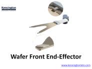
Kensington Robot End-Effectors have a long history of operation in semiconductor wafer fabrication. Several of Kensington’s End-Effector innovations have advanced wafer processing capability
| PowerPoint PPT presentation | free to download
The semiconductor industry is undergoing rapid growth, and silicon wafer manufacturing companies are key to this success. A silicon wafer is a thin piece of semiconductor material used in the fabrication of integrated circuits.
| PowerPoint PPT presentation | free to view
wafer cassette mapping sensor offers a cost-effective and reliable detection of slotting errors in cassettes or FOUPs. This mapper can detect any double-, empty- and cross-slotted status and wafer-misplacement.
| PowerPoint PPT presentation | free to download
In a process known as silicon Wafer Inspection and cleaning, particles on the surface must be removed from the surface. The process of silicon Wafer Polishing starts with removing any defects. If new material is used to produce a silicon wafer, it can create roughness on the surface. This is an important step in the process before a wafer reaches the fabrication facility (fab).
| PowerPoint PPT presentation | free to view
The Wafer front end production process gets done, the wafers are then transmitted to the assembly facility to save the chip.
| PowerPoint PPT presentation | free to download
According to the latest research report by IMARC Group, The global e-beam wafer inspection system market size reached US$ 759.9 Million in 2023. Looking forward, IMARC Group expects the market to reach US$ 3,459.6 Million by 2032, exhibiting a growth rate (CAGR) of 17.8% during 2024-2032. More Info:- https://www.imarcgroup.com/e-beam-wafer-inspection-system-market
| PowerPoint PPT presentation | free to download
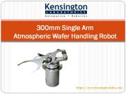
Kensington Laboratories 300mm single arm atmospheric wafer handling robot, part of the MultiLink™ robot family, is designed to meet the industry’s most rigorous 300mm performance standards.
| PowerPoint PPT presentation | free to download
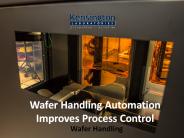
The wafer handling automation has become a powerful & convenient approach to protect the silicon wafers from the dust elements or small microns that plays a vital role in blocking the structure and halts up the overall performance of electronic devices.
| PowerPoint PPT presentation | free to download
The wafer handling robots are utilized in the semiconductor equipment spectrum for various processes such as thermal processing systems, deposition systems, metrology systems, and many more in any case.
| PowerPoint PPT presentation | free to download
In the fast-paced semiconductor manufacturing industry, optimizing yield and maintaining high-quality standards are paramount. As integrated circuits continue to shrink in size and increase in complexity, the necessity for precise, advanced methodologies becomes ever more critical. Among the technologies employed, wafer map software stands out as an indispensable tool. Leveraging complex algorithms, color-coded grids, and innovative software functionalities, advanced wafer mapping enables real-time analysis of semiconductor wafers at an unparalleled level of detail. This technology has dramatically transformed the industry, providing insights into defect patterns, yield calculations, and testing processes, hence enhancing semiconductor manufacturing efficiency and productivity. This blog delves into the intricacies of wafer mapping, exploring its role, advancements, and impact on semiconductor manufacturing.
| PowerPoint PPT presentation | free to download
Kensington Laboratories, the technology leader in semiconductor wafer handling automation products demonstrates their 300mm wafer handling robot.
| PowerPoint PPT presentation | free to download
Wafer Handling automation is used to restraint the silicon wafers from dust elements or small microns, which helps in blocking the structure and halts the overall performance of the electronic devices.
| PowerPoint PPT presentation | free to download
Purchase of Wafer AlignerBonder
| PowerPoint PPT presentation | free to download
The wafer front end semiconductors offer great compatibility for high-temperature applications. When it comes to taking care of the transparent substrate through beams, the semiconductor wafer front end-effectors help in achieving a lot in all sorts of needs.
| PowerPoint PPT presentation | free to download
300mm single arm atmospheric wafer handling robot, part of the Multilink robot family, is designed to meet the industry most rigorous 300mm performance standards. The Multilink Single Arm robot incorporates a host of unique, proprietary design features which combine to provide unsurpassed reliability, superior performance, and high throughput.
| PowerPoint PPT presentation | free to download
The innovative functionalities of wafer handling equipment & stage repair are the one-stop solutions to increase the performance of semiconductors.
| PowerPoint PPT presentation | free to download
Kensington Labs 300mm capable Multilink Dual Arm atmospheric wafer handling robot meets the industry most rigorous 300mm performance standards. The Dual Arm robot achieves extremely high throughput in a small footprint, providing a significant cost of ownership advantage.
| PowerPoint PPT presentation | free to download
The innovative functionalities of wafer handling equipment, stage repair precision control system and wafer cassette mapping are the end-to-end solutions to boost the semiconductors' performance.
| PowerPoint PPT presentation | free to download
According to the latest research report by IMARC Group, The global e-beam wafer inspection system market size reached US$ 631.3 Million in 2022. Looking forward, IMARC Group expects the market to reach US$ 1,921.1 Million by 2028, exhibiting a growth rate (CAGR) of 21.44% during 2023-2028. More Info:- https://www.imarcgroup.com/e-beam-wafer-inspection-system-market
| PowerPoint PPT presentation | free to download
The semiconductor industry, with its rapid technological progression and intricate manufacturing processes, relies heavily on precision and control for optimum yield. In this sphere, an element that has become crucial to maintaining high-quality standards is advanced wafer mapping. By harnessing state-of-the-art algorithms, distinctive color-coded grids, and innovative software features, wafer mapping software furnishes a high-resolution analysis of semiconductor wafers in real time. This capability, in turn, boosts the efficacy and output of the semiconductor manufacturing industry. The ensuing discussion elucidates the fundamentals and advancements in wafer mapping, spotlighting its crucial role in semiconductor production.
| PowerPoint PPT presentation | free to download
Once the impurities are treated with heat, the remaining material is 99% pure silicon. In order to make fine thin silicon wafer CA which are capable of transmitting weak electric signals, the remaining 1% impurities also have to be removed. Only those Silicon Wafers Manufacturing CA are distributed which pass the testing phase.
| PowerPoint PPT presentation | free to download
Scheduling of Wafer Fabrication Facilities using ... fixture changing program loading parameter tuning etc. Wafer Fab Scheduling Wafer fab is a very ...
| PowerPoint PPT presentation | free to view
We manufacture and supply the good quality plain cone, wafer cone and plain wafer cone, the crunchy and crispy, made in technologically advanced fully automatic plant.
| PowerPoint PPT presentation | free to download
Wafer cleaning just like Wafer Mapping has long been acknowledged as a significant industry procedure. It consists of the removal of particulate & chemical contaminations from the semiconductor surface without generating any harm to the substrate.
| PowerPoint PPT presentation | free to download
OPTI 521 Tutorial Presentation. 10. 6/27/09. System Components -computer ... Industrial computers, touchscreen control monitors. OPTI 521 Tutorial Presentation ...
| PowerPoint PPT presentation | free to view
Reticles and Mask. Reticle -a 'hard copy' of the individual drawing recreated in a thin layer of ... Masks and reticles are similar in makeup. ...
| PowerPoint PPT presentation | free to view
Looking forward, the e-beam wafer inspection system market value is projected to reach a strong growth during the forecast period (2021-2026). More info:- https://www.imarcgroup.com/e-beam-wafer-inspection-system-market
| PowerPoint PPT presentation | free to download
Kensington Laboratories is a leading supplier of wafer handling robots, precision motion control, integrated stages, linear stages and rotary stages. Contact Kensington for proven, robust products and automation solutions to enhance the performance.
| PowerPoint PPT presentation | free to download
The report of GaN device and wafer market identifies the entire market and all its sub-segments through extensively detailed classifications, in terms of revenue, shipments and ASPs. This market report has detailed research study on GaN market with respect to devices and substrate wafers.
| PowerPoint PPT presentation | free to download
Reticle. Lens. Reticle. Wafer. Design. ASML Procurement. Means & Methods / Slide 12 ... Reticles. Lenses. Handlers/stages. Lasers. Optics. Wafers. Fasteners ...
| PowerPoint PPT presentation | free to view
... formation of metal oxide and nitride thin films chemical vapour deposition chemical vapour deposition diapositiva 7 metal organic chemical vapor deposition, ...
| PowerPoint PPT presentation | free to view
1. Coat a 50mm diameter quartz wafer with 0.3 m of polysilicon followed by a 8 ... Quartz annulus. Slots. Freestanding Cu FSS. Quartz annulus. Electroplated Cu ...
| PowerPoint PPT presentation | free to view
Wafer Acceptance Testing (WAT) and Process Control Monitoring (PCM) are instrumental elements within the semiconductor manufacturing industry. They are crucial tools utilized predominantly by fabless companies that seek to monitor and enhance their yield and defect rates. WAT/PCM is the systematic measurement of various device parameters during different stages of wafer processing. It establishes control over the manufacturing process, leading to better consistency and quality of the final product. This measurement process aims to build a comprehensive database of process information, useful for a variety of process enhancement and control activities.
| PowerPoint PPT presentation | free to download
Multi-Project Reticle Floorplanning and Wafer Dicing. Andrew B. ... Reticle floorplanning and wafer dicing problem. Conclusions and future research directions ...
| PowerPoint PPT presentation | free to download
Crystallizing dishes marked for sulfuric acid and hydrogen peroxide are used to clean the wafers Place wafer into ... Begin deposition Record pressure at start ...
| PowerPoint PPT presentation | free to download
Kensington EFEN equipment enables easy integration of different devices, like Prealigners, Robotics, Wafer ID readers, Load Ports, and several other devices.
| PowerPoint PPT presentation | free to download
MEMS Example Micralyne MEMS Example NASA LCROSS MEMS Compared to ICs Similarities: Wafer fabrication with common materials and fabrication methods Silicon wafers ...
| PowerPoint PPT presentation | free to view
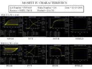
MOSFET IV CHARACTERISTICS Lot Number = F050118 Wafer Number = D4 Date = 11-13-2006 Process = SMFL CMOS Product = DAC03 NMOS L/W = 4/16
| PowerPoint PPT presentation | free to download
Si is oxidised by oxygen or steam at high temperature according to the following ... Wafer cleaning station. Wafer load station. Process automation. Vertical ...
| PowerPoint PPT presentation | free to view
In the fast-paced world of semiconductor manufacturing, preventing process excursions is crucial for optimizing yield, reducing wafer scraps, and efficiently allocating engineering and manufacturing resources. The prevention of process excursions is of utmost importance in the semiconductor manufacturing industry as it directly impacts yield loss, wafer scraps, and the efficient allocation of engineering and manufacturing resources.
| PowerPoint PPT presentation | free to download
The XYZ precision stage is designed by combining three existing DOF motion stages via nested structure. Through the use of previously developed stages, this approach has apparently decreased the effort for the design and analysis steps and offer reasonable reliability. For more information, check out the presentation.
| PowerPoint PPT presentation | free to download
M. Garcia-Sciveres - ATLAS Pixel Review - Module Assembly. 2. The ... Wafer thinning: Okamoto (Bay Area) Wafer dicing: various qualified vendors (Bay Area) ...
| PowerPoint PPT presentation | free to download


