Wafer Front End PowerPoint PPT Presentations
All Time
Recommended
The semiconductor industry is improving daily, either for the production equipment manufacturers or the end-users. In fact, the transistors in the integrated circuit are getting increased along with the performance.
| PowerPoint PPT presentation | free to download
Kensington Robot End-Effectors have a long history of operation in semiconductor wafer fabrication. Several of Kensington’s End-Effector innovations have advanced wafer processing capability
| PowerPoint PPT presentation | free to download
The Wafer front end production process gets done, the wafers are then transmitted to the assembly facility to save the chip.
| PowerPoint PPT presentation | free to download
The wafer front end semiconductors offer great compatibility for high-temperature applications. When it comes to taking care of the transparent substrate through beams, the semiconductor wafer front end-effectors help in achieving a lot in all sorts of needs.
| PowerPoint PPT presentation | free to download
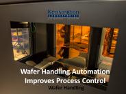
Wafer Handling automation is used to restraint the silicon wafers from dust elements or small microns, which helps in blocking the structure and halts the overall performance of the electronic devices.
| PowerPoint PPT presentation | free to download
The order arrival rate, the average order size, batching policy, automated material wafer handling system, and the number of batch tools significantly affect the models' performance. Read this ppt to get more information.
| PowerPoint PPT presentation | free to download
The Semiconductor front end device fabrication is the procedure to generate the integrated circuits that have electrical and electronic devices.
| PowerPoint PPT presentation | free to download
Wafer cassette mapping and wafer front end are going to help you make the most out of your business. To locate the provider rendering a wide variety of good quality wafer cassettes mapping services, you need to make sure to look out for some real pros. Let's check out the PPT for more info.
| PowerPoint PPT presentation | free to download
EVLA FrontEnd CDR FrontEnd Production Plans
| PowerPoint PPT presentation | free to download
Title: No Slide Title Author: Dan Ferrin Last modified by: International SEMATECH Created Date: 5/25/2001 6:12:52 PM Document presentation format
| PowerPoint PPT presentation | free to view
Kensington Laboratories offers Performix, a 300mm equipment front-end module (EFEM) wafer handling environment designed for ISO Class 1 specification, to address the growing constraints faced by the semiconductor industry.
| PowerPoint PPT presentation | free to download
Kensington EFEN equipment enables easy integration of different devices, like Prealigners, Robotics, Wafer ID readers, Load Ports, and several other devices.
| PowerPoint PPT presentation | free to download
DRAFT Work In Progress - NOT FOR PUBLICATION 13 July 2005. Front End Processes ... Allowable defect densities for HP MPU consider new chip size scenario in 2005 ...
| PowerPoint PPT presentation | free to view
Lecture 19 ASIC Front-End Design ... CMOS technology implies that all active devices, or transistors, come in pairs of N- and PMOS transistors.
| PowerPoint PPT presentation | free to view
Are you looking for wafer robot repair solutions? Kensington Laboratories offers certified products of precision handling robots to stage repair programs that can help smooth out industry operations and offer you value for money.
| PowerPoint PPT presentation | free to download
What are you waiting for when you can get the authentic products of the stage repair, semiconductor front end robots at a very affordable rate? Consult our team today and get the required solutions for your businesses.
| PowerPoint PPT presentation | free to download
With the rising alterations in the market, the semiconductor's differential production is emerging to be a strong dependency on the robotic wafer handling industry. It is one of the most reputed and demanding manufacturing processes with the implementation of robotics.
| PowerPoint PPT presentation | free to download
A number of ASICs have been designed for experiments at LHC, FNAL, BNL, etc. ... Other ASICs will become available in the near future (i.e., CARIOCA) and may be ...
| PowerPoint PPT presentation | free to view
Front-End electronics for Future Linear Collider W-Si calorimeter physics prototype ... 12 FLCPHY3 front-end chip. 18 ... Front-end board. 30 march 2004 ...
| PowerPoint PPT presentation | free to download
9-13 Sept. 2002 LECC2002. 1. Christine HU-GUO. Test and Evaluation ... Designed on a deep submicron 0.25 mm process. For safety margins in radiation environment ...
| PowerPoint PPT presentation | free to download
Title: PowerPoint Presentation Author: Ian Lazarus Last modified by: Ian Lazarus Created Date: 7/8/2005 2:23:58 PM Document presentation format: On-screen Show
| PowerPoint PPT presentation | free to download
Title: A view on electronics for the prototype of the TimePix detector in 0.13um CMOS Technology. Author: vgromov Last modified by: vgromov Created Date
| PowerPoint PPT presentation | free to download
Correlate in-line chamber metrology with gas panel testing ... Replenish printer cartridges and paper. Train staff to use the tester. Use the tester ...
| PowerPoint PPT presentation | free to view
Broad-band and Scalable Circuit-level Models of MSM PD for Co-design with Preamplifier in Front-end Rx Applications ...
| PowerPoint PPT presentation | free to download
Title: PowerPoint Presentation Last modified by: Created Date: 1/1/1601 12:00:00 AM Document presentation format:
| PowerPoint PPT presentation | free to download
The semiconductor front end wafer handling robots have increased performance demands, and require high accuracy and reliability for driving mechanical constraints.
| PowerPoint PPT presentation | free to download
Title: PowerPoint Author: chk Last modified by: adminastor Created Date: 5/2/2000 8:48:20 AM Document presentation format: A4 (210x297 )
| PowerPoint PPT presentation | free to download
... areas in the front-end-of-line (FEOL) wafer fabrication ... Front End Etch Processes-Tables 34a&B, Figure 21. Transistor Doping-Tables 34a &b, Figure 20 ...
| PowerPoint PPT presentation | free to view
... Becomes e2v semiconductors Grenoble Industrial Facilities Wafer Fab Front-end Class 10 and 1 clean rooms CCD technology CMOS imager and sensor post ...
| PowerPoint PPT presentation | free to download
Gerd J. Kunde. FPIX2 Status. Produced 3168 chips in engineering run ... Gerd J. Kunde. PHX Cost. Chip design/testing 2 man-years - $275K (includes all ...
| PowerPoint PPT presentation | free to download
Have done one wafer using Atmospheric Discharge Plasma technique that is a non-contact method aimed specifically at thin bumped wafers(SmartCard market).
| PowerPoint PPT presentation | free to download
The wafer handling automation has become a powerful & convenient approach to protect the silicon wafers from the dust elements or small microns that plays a vital role in blocking the structure and halts up the overall performance of electronic devices.
| PowerPoint PPT presentation | free to download
Introduction CAD tools ... Where does the Gate Level Netlist come from? 1st Input to Astro Standard Cell Library 2nd Input to Astro Basic Devices and ...
| PowerPoint PPT presentation | free to view
Automated wafer handling has reduced throughput time and increased the efficiency and yield of wafer cassette mapping. To know more, check out the short presentation.
| PowerPoint PPT presentation | free to download
300mm single arm atmospheric wafer handling robot, part of the Multilink robot family, is designed to meet the industry most rigorous 300mm performance standards. The Multilink Single Arm robot incorporates a host of unique, proprietary design features which combine to provide unsurpassed reliability, superior performance, and high throughput.
| PowerPoint PPT presentation | free to download
Front Opening Unified Pods Market
| PowerPoint PPT presentation | free to download
The innovative functionalities of wafer handling equipment & stage repair are the one-stop solutions to increase the performance of semiconductors.
| PowerPoint PPT presentation | free to download
Front Opening Unified Pods (FOUP) Market
| PowerPoint PPT presentation | free to download
Gerd J. Kunde. PHENIX Silicon Endcap Physics. Open Beauty ... Gerd J. Kunde. Si Umbrella Layout. 50 mu radial pitch (z ... Gerd J. Kunde ...
| PowerPoint PPT presentation | free to download
Minor tweaking of design needed before production ... Simulated 1st and 2 nd stage. risetime (10-90%) with. different detector capacitance ...
| PowerPoint PPT presentation | free to download
Front End Electronics. Principal components: QIE (charge integrator and encoder) Fermilab ASIC ... Front-end electronics are on schedule ...
| PowerPoint PPT presentation | free to view
A wafer thin shell of porcelain that is cemented onto the front of the teeth to cover up the imperfection
| PowerPoint PPT presentation | free to download
Kensington Laboratory aims to craft the most innovative, dependable, and outstanding wafer handling robots, ADOs, end-effectors, FOUP opener and pre-aligners at an affordable rate.
| PowerPoint PPT presentation | free to download
Kensington Laboratory aims to craft the most innovative, dependable, and outstanding wafer handling robots, ADOs, end-effectors, FOUP opener and pre-aligners at an affordable rate.
| PowerPoint PPT presentation | free to download
RPC Front End Electronics. On chamber discriminator. The strips. The CMS discriminator chips ... Cable routing space needed in front of the crate. STATUS ...
| PowerPoint PPT presentation | free to download
... IZM-Berlin, Tyndall Institute, Heriot Watt University, Lancaster University/UK ... New concept built on a 30k funded project with Heriot Watt and IMEC ...
| PowerPoint PPT presentation | free to view
PCB to hold chips and silicon wafers under design, production in 2003. Custom-built VME ... for any/all options Back-end electronics ... custom RPC plane ...
| PowerPoint PPT presentation | free to download
Couple SLAC's front-end and electronics design capability to ... Camera. Scattered. Photons. With: Diamond Light Source, Hawaii, Molecular Biology Consortium ...
| PowerPoint PPT presentation | free to view
Register Alias Table (RAT) consulted ... A delta register (ESPD) is maintained in the front end ... Execution Unit into the renamed register during stage 83 ...
| PowerPoint PPT presentation | free to view
Global semiconductor manufacturing equipment market was valued at USD 95.3 billion in 2021 and is projected to reach USD 175.0 billion by 2027; it is anticipated to register a CAGR of 8.5% during the forecast period. Browse 302 market data Tables and 79 Figures spread through 364 Pages and in-depth TOC on "Semiconductor Manufacturing Equipment Market with COVID-19 Impact Analysis by Front-end Equipment, Back-end Equipment, Fab Facility Equipment, Product Type, Dimension, Supply Chain Participant, Region - Global Forecast to 2027"
| PowerPoint PPT presentation | free to download
Shown here are cables from both front and back sides of the pixel module. ... HDI/Ribbon Cable Flexor. One end is at -10C, and one at 25C to cool the power lines. ...
| PowerPoint PPT presentation | free to download
All timing and control to very front-end board via fibre-optic cables ... A critical issue in final system is cross-talk and pick-up in 1.6m kapton cables ...
| PowerPoint PPT presentation | free to download
One ABCD chip was not correctly glued. As a result, the bonds touch the edge ... In green, the sum of the front and back wafer after they have been glued to the spine ...
| PowerPoint PPT presentation | free to view
Each gives analogue signal, 14-bit dynamic range. Very-front-end (VFE) ASIC (Orsay) ... Firmware stored on CompactFlash card; replacing this also works ...
| PowerPoint PPT presentation | free to view
Each gives analogue signal, 14-bit dynamic range. Very-front-end (VFE) ASIC (Orsay) ... Firmware stored on CompactFlash card; replacing this also works ...
| PowerPoint PPT presentation | free to download


