
Schottky PowerPoint PPT Presentations
All Time
Recommended
Anneal sample as before (1600 for 30 min) Remove Carbon Cap (RIE with O2) ... Channel mobility: 40- 45 cm2/Vs (on epilayer layer annealed at 1600 C) Stable up to 15V ...
| PowerPoint PPT presentation | free to download

Schottky diode is also known as barrier diode. Learn more about Schottky diode working, construction, V-I characteristics, features and applications
| PowerPoint PPT presentation | free to download

Big Market Research added a new research report on "2015 Schottky Diode Industry Report - Global and Chinese Market Scenario" Read Complete Report on: http://www.bigmarketresearch.com/schottky-diode-industry-2015-global-and-chinese-analysis-market 2015 Schottky Diode Industry Report - Global and Chinese Market Scenario is an expert and top to bottom business sector study on Global and Chinese Schottky Diode industry. The report firstly surveys the fundamental data of Schottky Diode including its characterization, application and fabricating innovation.
| PowerPoint PPT presentation | free to download

The 'Global and Chinese Schottky Diode Industry, 2010-2020 Market Research Report' is a professional and in-depth study on the current state of the global Schottky Diode industry with a focus on the Chinese market. Request a sample of this report @ http://www.orbisresearch.com/contacts/request-sample/37147 Browse the full report @ http://www.orbisresearch.com/reports/index/global-and-chinese-schottky-diode-industry-2010-2020-market-research-report
| PowerPoint PPT presentation | free to download

Schottky diode I-V characteristics Schottky diode is a metal-semiconductor (MS) diode Historically, Schottky diodes are the oldest diodes MS diode electrostatics and ...
| PowerPoint PPT presentation | free to download

BBQ parasitic to resonance compensation 'Mission Accomplished', but. ... Vert. I and Q. Tunes and beam decay. Horiz. I and Q. loss of lock. 17 Mar 2006. BBQ ...
| PowerPoint PPT presentation | free to download

This algorithm is realized in MathCad. ... The MathCad code looks ready for translation into a routinely working console application. ...
| PowerPoint PPT presentation | free to view

548 Microelectronic Device Fabrication. 549 Analog Integrated Circuits Layout. 553 Microelectronic Fabrication Laboratory. Physics of PN, Schottky (MS), and ...
| PowerPoint PPT presentation | free to view

for wavelength of 8-10 m. Conclusion. 4. Laser types and covered ... Shorter wavelength, l~7.8 mm (larger confinement GAR, smaller losses aw) Improved design: ...
| PowerPoint PPT presentation | free to view

R.Siemann USPAS lectures: (1992S) Topics in Experimental Accelerator Physics. W. Mackay USPAC lectures: (2005S) Accelerator Physics Supplementary Notes ...
| PowerPoint PPT presentation | free to download

... Employ Schottky effect in the RF photocathode gun and with low energy photons This technique may produce an electron beam with ultra-low intrinsic emittance ...
| PowerPoint PPT presentation | free to view

Of A Different Construction. Photoconductive Cell. LCD (Liquid-Crystal Display) Thermistor ... Max VF @ IFM = IO. 125 C. TJ Max. 50. 75. 85. TC @ Rated IO ( C) ...
| PowerPoint PPT presentation | free to view

Development of SiC Schottky Diode Detectors as an Advanced Sensor for Safeguards ... Develop SiC Schottky diode detectors for measurement of actinide concentrations, ...
| PowerPoint PPT presentation | free to view

Design and optimization of Schottky diodes in CMOS technology with application ... F.M. Gerrits, etc. Centre Suisse d'Electronique et de Microtechnique SA (CSEM) ...
| PowerPoint PPT presentation | free to view

Towards Spintronics: Measurement of Schottky barriers of iron on silicon films ... semiconductor interfaces have an energy barrier called the 'Schottky Barrier' ...
| PowerPoint PPT presentation | free to download

Auto-ID lab Adelaide. Overview. Introduction. Design and layout of Schottky diode. ... sources of diversion, identify counterfeiting, theft prediction, faster recalls ...
| PowerPoint PPT presentation | free to view

Experimental Results on Bunched Beam Schottky Signals and Possible Implications ... 2 GHz for the Tevatron has been designed in 1987 (Goldberg et al, LBL 22273) ...
| PowerPoint PPT presentation | free to download

FIG 1: SKPM surface potential traces next to a Schottky contact with an 8 V ... present on a-plane GaN, we must attribute such band bending to the presence of ...
| PowerPoint PPT presentation | free to download

Contact M tal Semi-conducteur Diode Schottky Contact M tal/SC: diode Schottky Plusieurs applications: Interconnexions Contact Ohmique Diode barri re Schottky ...
| PowerPoint PPT presentation | free to download

Metal - Semiconductor junction are used for high speed rectification. Simulation of Schottky diodes. Schottky diodes are formed in two ways: ...
| PowerPoint PPT presentation | free to view

Fermi-Level Pinning & Schottky Barrier Height B93501044, B93505007 * Schottky Barrier Ideal Condition m: The ...
| PowerPoint PPT presentation | free to download

Diode semiconductor Tunnel, Gunn, Impatt, Varactor diodes, PIN, LSA, Schottky barrier diode. 4.1.1 MICROWAVE TUBES Used for high power/high frequency combination.
| PowerPoint PPT presentation | free to download

This article discusses about types of transistors and basic applications.Common types of transistor are BJT, FET, HBT, Darlington, Schottky, JFET, Diffusion
| PowerPoint PPT presentation | free to download

Temas Fen menos de Ruptura Juntura: Desviaciones de lo ideal Interfaces Metal-Semiconductor y Diodo Schottky Dispositivos Optoelectr nicos Referencias
| PowerPoint PPT presentation | free to download
Schottky barrier modulation. at the contacts. local ... neglect Schottky barrier. Charge injection from p-doped. CNT contacts. CNTFET control capacities ...
| PowerPoint PPT presentation | free to download

Diode in historisch perspectief Hans Wallinga Emeritus Universiteit Twente Vacu m Diode Schottky diode pn-overgang Fysische werking vacu m diode Thermische emissie ...
| PowerPoint PPT presentation | free to download
Schottky diodes, photodiodes, photo mixers, RTDs, ... high current density, ... S.R. Bank, NAMBE , 2006. Epitaxially formed, no surface defects, no Fermi level pinning ...
| PowerPoint PPT presentation | free to download

Enhancing the Electrical and Optoelectronic Performance of Nanobelt Devices by ... that act as 'transition states' and effectively reduce the Schottky barrier. ...
| PowerPoint PPT presentation | free to view

Voltage-controlled capacitance - varactor. Asymmetric junctions. Tuning voltage. metal ... Schottky Barrier. Built-in Field. x. N-type Schottky depletion ...
| PowerPoint PPT presentation | free to view

Frenquency measurement (by Schottky-Pickups) 2. The Experiment: ... Frenquency measurement (by Schottky-Pickups) due to cooling (?v/v 0), the fre ...
| PowerPoint PPT presentation | free to view
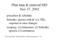
procedure & schedule. Schottky spectra with & w/o TEL, response to ... fit inverse parabola to segments to get the tune. Pbar and proton tunes. 0.5770 /-0.0003 ...
| PowerPoint PPT presentation | free to download

(imagine an analogy of Frenkel and Schottky Defects in solid state physics) Models for crystal growth Transport-controlled growth ...
| PowerPoint PPT presentation | free to download

Concept of Field Effect Transistor. 1947 Bipolar Transistor. Bipolar IC ... Schottky contact. Si2O. Microelectronics Processing Course J. Salzman Fall 2006. 14 ...
| PowerPoint PPT presentation | free to view

Fundamentals of Nanoelectronics Lecture 7 MESFETs Schottky Barrier Devices Heterojunction Transistor HEMTs * In Ga As/In P heterojunction References: Solid State ...
| PowerPoint PPT presentation | free to view

Metal-semiconductor (MS) junctions Many of the properties of pn junctions can be realized by forming an appropriate metal-semiconductor rectifying contact (Schottky ...
| PowerPoint PPT presentation | free to download

Fermi Energy. Energy Model for a Metal. Energy. Bulk electron. Donath, ... Fermi Energy. n-type. Metal-Semiconductor Interface. Schottky Barrier. Built-in Field ...
| PowerPoint PPT presentation | free to view

1.1 IR Detector Classification and Characteristics. 1.2 Present Status ... by the Schottky heterodyne princaple (SIS = superconductor-insulator ...
| PowerPoint PPT presentation | free to view
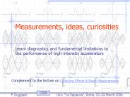
Complement to the lecture on Collective Effects & Beam ... Longitudinal Schottky scan spectrogram during debunching. Low-intensity beam. High-intensity beam ...
| PowerPoint PPT presentation | free to download

M. Steck, ICFA Workshop, October 18-22, 2004. Cooled Heavy ... ESR operation in isochronous mode t = 1.38. longitudinal Schottky signal. horizontal beam profile ...
| PowerPoint PPT presentation | free to view

Bharat Book Bureau provides the report, on “Global and China Automotive Semiconductor Industry Report, 2014-2015”. https://www.bharatbook.com/automotive-market-research-reports-711675/global-china-automotive-semiconductor.html Automotive power semiconductor mainly involves Power Management ICs, MOSFET, IGBT, and Diodes (Fast Recovery, Schottky, and High Voltage).
| PowerPoint PPT presentation | free to download

For example 7404, a TTL inverter chip. LSTTL: Low-power Schottky transistor-transistor logic. ... For example 74HC04, an HCMOS inverter chip. Definition of Terms 2 ...
| PowerPoint PPT presentation | free to view

Beam loss and longitudinal emittance growth in SIS. M. Kirk ... Fitting program: Ziemann, Svedberg Laboratory] Schottky spectrum under high phasespace density ...
| PowerPoint PPT presentation | free to view

Fm work function of metal. Fs work function of semiconductor ... hyperphysics.phy-astr.gsu.edu. Schottky junctions Thermionic Emission Theory. From previous page: ...
| PowerPoint PPT presentation | free to view

Full collaboration meeting April, LBL. Beam-beam compensation ... Deliver tune tracker, luminometer, Schottky. Mini collaboration meeting October, FNAL ...
| PowerPoint PPT presentation | free to download

Igual geometr a. Tres capas de aSi. Capas dopadas 10-20 nm. Irradiaci n con gammas ... Igual al test de gammas. Medidas de respuesta del sensor. Schottky vs dosis ...
| PowerPoint PPT presentation | free to view

Aliovalent impurities also introduce excess defects whose concentration is fixed ... Schottky defects. A cation vacancy an anion vacancy (Vm'Vx ...
| PowerPoint PPT presentation | free to view

GHz Schottky Pick-ups for LHC. Andreas Jansson. Fermilab. 5/8/09. Proton driver workshop ... Tune during store. Tune is extracted from location of betatron bands. ...
| PowerPoint PPT presentation | free to view

Estimation du taux de sursauts ? d tectables par an. Mod le de masse de la cam ra CXG ... 6084 d tecteurs CdTe Schottky (4 x 4 x 2 mm3) avec anneau de garde (0.5 mm) ...
| PowerPoint PPT presentation | free to view

D.U.T.. D.U.T.. 1N5822 or 1N5817. 1N4001. Schottky diode. Standard rectifier -- fool proof ... Need to protect your sensor from the rest of your circuit? ...
| PowerPoint PPT presentation | free to view

The temperature dependence performance of ultraviolet radiation detectors T. V. Blank, Yu. A. Goldberg, O. V. Konstantinov Ioffe Physico-Technical Institute
| PowerPoint PPT presentation | free to download

... makes metallic S/D SBMOS as one of the most attracting candidates for use ... noise behavior and mechanisms in SBMOS require further thorough investigations. ...
| PowerPoint PPT presentation | free to download

ECE 875: Electronic Devices Prof. Virginia Ayres Electrical & Computer Engineering Michigan State University ayresv@msu.edu
| PowerPoint PPT presentation | free to download

2 Novel Device Group, Intel Corporation, Hillsboro, OR ... favorable device characteristics. Vtip = -2V ... ambipolar transfer characteristic (I vs Vg) ...
| PowerPoint PPT presentation | free to download
... entire light sensitive area Phototransistor High gain through the transistor action Slower response-time compared with photodiode pn-diode 0.01us Ph-trans. 5 ...
| PowerPoint PPT presentation | free to download

The term metal-silicon contact includes silicide-Si contacts. The semiconductor is depleted of mobile carriers to a depth W In the depleted region (0 ...
| PowerPoint PPT presentation | free to download

3 Diode * EEE270 Electronic engineering EEE270 Electronic engineering EEE270 Electronic engineering EEE270 Electronic engineering EEE270 Electronic ...
| PowerPoint PPT presentation | free to view