JAVA Applets for Physical Electronics. - PowerPoint PPT Presentation
1 / 15
Title:
JAVA Applets for Physical Electronics.
Description:
Metal - Semiconductor junction are used for high speed rectification. Simulation of Schottky diodes. Schottky diodes are formed in two ways: ... – PowerPoint PPT presentation
Number of Views:115
Avg rating:3.0/5.0
Title: JAVA Applets for Physical Electronics.
1
JAVA Applets for Physical Electronics.
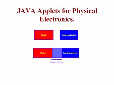
Metal
Semiconductor
Metal
Semiconductor
Depletion Region
2
Team Members
- Team Leader/Presentation
- Ramya Chandrasekaran
- Webmaster/Documentation
- Pujita Pinnamaneni
3
Project Goal
- Design a JAVA Applet to help students understand
the characteristics of Schottky diodes. - Demonstrate the energy band gap and depletion
width variations for varying concentrations and
for different metals and semiconductors. - Demonstrate how the free carrier concentration
varies with temperature.
4
Project Outline
- Review semiconductor physics of Schottky diodes.
- Develop simulation for band gap variation with
respect to concentration for different metals and
semiconductors. - Develop simulation of n/ND and p/NA
vs.temperature.
5
Project Outline(cont.)
- Develop JAVA code to run these simulations.
- Design JAVA applets.
- Demonstrate the applets.
- Launch the Applets on the World Wide Web.
6
Importance of JAVA Applets
- JAVA enables to develop user friendly
applications. - JAVA is the web language.
- Enables easy interaction .
- GUI concepts in JAVA accepts user inputs through
mouse and keyboard and enables immediate
feedback. - Animations and interactive applications are
possible.
7
Importance of Schottky diodes
- The role of schottky diodes is firmly established
in the semiconductor technology because they
perform functions better than most of the other
junction devices. - These contacts are used in large number of
devices such as FETs,BJTs,photo
detectors,LEDs,Double Heterostructure lasers and
Solar cells. - Metal - Semiconductor junction are used for high
speed rectification.
8
Simulation of Schottky diodes.
- Schottky diodes are formed in two ways
- Metals deposited on n-type semiconductor.
- Metals deposited on p-type semiconductor.
9
Schottky Contacts.
- In n-type Schottky contacts,electrons flow from
the conduction band states in the semiconductor
to the metal because they have higher energy
states. - In p-type Schottky contacts,electrons flow from
the metal to semiconductor.
10
Metal on n-type Semiconductor
11
Metal on p-type Semiconductor.
12
Temperature Vs Free carrier Concentration
- The regions on the curve are
- Freeze-out
- Depicts the unionized dopants
- Extrinsic Region
- Represents ionized dopants and control
conductivity. - Intrinsic Region
- Characterizes broken covalent bonds
13
Basic Principles(cont)
14
Physics Involved
- The intrinsic carrier concentration is calculated
- ni nio (T/To)1.5 exp (Eg / 2KTo) (1-
To/T) - ND1 ( Nd1/ (12Nd1/(NCO ni1.5) ) exp (( Ec
Ed1)/KT)
15
Conclusions
- Simulation of Schottky diodes using JAVA Applets
is accomplished. - Temperature Vs. Free carrier concentration curves
for different semiconductors have been plotted. - Applets have been successfully hosted on the
World wide web.


