Nanofabrics PowerPoint PPT Presentations
All Time
Recommended
Routing for Reliability in Molecular Diode-based Programmable Nanofabrics Kushal Datta, Arindam Mukherjee and Arun Ravindran Department of Electrical and Computer ...
| PowerPoint PPT presentation | free to download
Strategy: substitute compile time (cheap) for manufacturing precision (expensive) ... 100x speedup when compiled properly. Do not do speculative or parallel ...
| PowerPoint PPT presentation | free to view
BY MERCY N' OFFOR, PhD'
| PowerPoint PPT presentation | free to view
Specialized Functional Elements and Processing Elements ... First handling some touch-pad interaction, next doing video processing ...
| PowerPoint PPT presentation | free to view
Spatial Computation. A computation model based on: application ... HW compilation for spatial computation. Studied first-order properties of spatial computation ...
| PowerPoint PPT presentation | free to download
A Hybrid CMOS/NAnoTUbe REconfigurable Architecture. Motivation. Background on CNT and NRAM ... Lack of a mature fabrication process. Defects and run-time failures ...
| PowerPoint PPT presentation | free to view
A Probabilistic Approach to Nano-computing. J. Chen, J. Mundy, Y. Bai, S.-M. C. Chan, ... Nano-scale devices are attractive but have high probability of failure ...
| PowerPoint PPT presentation | free to download
Join forces of LCCC and Technical High Schools. to maximize resources. to ... Cosmetology. Culinary Arts. Health Occupations. Medium Heavy Truck Technology ...
| PowerPoint PPT presentation | free to view
Focused Ion Beam Market
| PowerPoint PPT presentation | free to download
Focused Ion Beam Market
| PowerPoint PPT presentation | free to download
Guires FRL offers end-to-end nutraceuticals & supplement contract R&D product innovation & manufacturing solutions to companies worldwide.
| PowerPoint PPT presentation | free to download
Fabricate ordered arrays of structures on the nanometer scale using porous alumina templates. ... Why do we want to fabricate nanostructures? ...
| PowerPoint PPT presentation | free to download
Global Focused Ion Beam (FIB) Market is estimated to reach $530 million by 2024; growing at a CAGR of 6.8% from 2016 to 2024. Focused Ion Beam is an advanced technique majorly used in industries such as materials science, semiconductor, and others. Currently, FIB systems are commonly found in a broad range of applications in medical science laboratories. FIB technique has also gained popularity in the biological field for deposition, ablation of materials, and site specific analysis. Global-Focused-Ion-Beam-Market-Size-and-Forecast-2015-2024-(US$-Million)
| PowerPoint PPT presentation | free to download
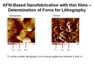
AFM-Based Nanofabrication with thin films Determination of Force for Lithography topography friction 7 v 8 v 9 v 7 v 8 v 9 v To achieve better lithography, force ...
| PowerPoint PPT presentation | free to download
Nanotechnology Leaping with tiny Steps into the Future
| PowerPoint PPT presentation | free to download
... aa Ga G G GpGpSa GpGSsGpS pSsGSs spSs tpS tSs tFpstFSs t tFS FS tFT F tFTs tTFTO tOdFTOFTd ... e tftett FeFFF TeTTT OOeOO Odeddd efeff ffee ee n C ...
| PowerPoint PPT presentation | free to view
Steven Ross. Katharine Tull. Maryam Attari. Tim Beach. Greg Hidley ... Steven Ross sross@ucsd.edu 858-822-3072. Katharine Tull, ktull@ucsd.edu 858-822-4108 ...
| PowerPoint PPT presentation | free to download
Partnership for Regional Innovation in Manufacturing Education Dr. Pearley Cunningham Co-Principle Investigator - PRIME Department Head Engineering Technology
| PowerPoint PPT presentation | free to view
NANO 230 Micro/NanoFabrication Scanning Electron Microscopes *
| PowerPoint PPT presentation | free to view
Prof. Enrico Gratton - Lecture 6 - Part 1. Fluorescence Microscopy ... HBO 50W/AC. HBO 100W/2. High-pressure Mercury lamps. Lifetime (h) Arc size. h x w (mm) ...
| PowerPoint PPT presentation | free to download
BioMEMS for Instrumenting and Controlling the Single Cell
| PowerPoint PPT presentation | free to download
'If I were asked for an area of science and engineering that ... Harrisburg Area Community. College. Lehigh Carbon Community. College. Luzerne County Community ...
| PowerPoint PPT presentation | free to download
Properties of nano-sized structures are different from their bulk and molecular counterparts. ... The two most important conditions are narrow voltage ranges ...
| PowerPoint PPT presentation | free to download
Nanomaterials in Construction and Rehabilitation: Contributions and Perspectives of the US National
| PowerPoint PPT presentation | free to download
EE143 Microfabrication Technology Professor: Ali Javey ajavey@eecs.berkeley.edu 506 Cory Hall (510) 643-7263 TAs: SangHoon Lee, leesh@me.berkeley.edu
| PowerPoint PPT presentation | free to download
Heavy use of Hands-on Activities ... West Mifflin, PA 15122. Phone (412) 469-6299. email: pcunningham@ccac.edu. http://www.ccac.edu or ...
| PowerPoint PPT presentation | free to download
... www.w3.org/1999/02/22-rdf-syntax-ns#' xmlns:iX='http://ns.adobe.com/iX/1.0 ... xmlns:xapMM='http://ns.adobe.com/xap/1.0/mm ...
| PowerPoint PPT presentation | free to download
Collaboration with Industry and Other Sectors Summary of C-SPIN Partnerships Texas Instruments Collaboration International Collaborations Santos and Murphy - NTT and ...
| PowerPoint PPT presentation | free to download
Single Molecule Electronics And NanoFabrication of Molecular Electronic Systems
| PowerPoint PPT presentation | free to download
Bill Schultz. Program Director, Fluid Dynamics and Hydraulics, University of Michigan ... Lawrence Goldberg. Electronics, Photonics and Device Technologies ...
| PowerPoint PPT presentation | free to view
California Institute for Telecommunications and Information Technology ... Evolving a System Requires Knowing the Initial State ...
| PowerPoint PPT presentation | free to download
Fabrication. After patterning a masking layer, a reactive ion ... herein an approach to fabricate silicon nanostructures with controllable sidewall profiles. ...
| PowerPoint PPT presentation | free to download
Plasmonic excitations in nanostructured materials. Cristian Kusko and Mihai Kusko ... Metamaterials and Left Handed Metamaterials (LHM)? n 0; e 0; m 0 ...
| PowerPoint PPT presentation | free to download
... Sturm, and R. H. Austin, Deterministic hydrodynamics: taking blood apart, Proc. ... Sturm, Determining blood cell size using micro?uidic hydrodynamics, J. Immunol. ...
| PowerPoint PPT presentation | free to download
Overview of Nanofabrication Material depostion methods Thin films of materials Thickness measurement Lithography Pattern transformation on to planar suface
| PowerPoint PPT presentation | free to view
[181 Slide] Service Laboratory Market analysis & forecast report categorizes global market by Service Type (OEM, Laboratory Services), Product/Technology (FE-TEM, STEM, FIB-SEM, FEG-SEM, SIMS), Application (Biotechnology, Pharmaceutical, Semiconductor) and Geography (North America, Europe, APAC) & Geography.
| PowerPoint PPT presentation | free to download
Laser Physics Centre, Department of Physics, University of Queensland ... William Belcher. Eliecer Para. Geoff Leech* DeborahLouGreig. Ming Sheng Liu. Glenn Moloney ...
| PowerPoint PPT presentation | free to download
Nanostructures - PNPA NANO51 Foothill College Glasses Nanostructured glasses have areas that are glass and areas that are interfacial (this is controlled by the ...
| PowerPoint PPT presentation | free to download
NANOROBOTICS. [2] NANOFABRICATION. NANOMECHANICAL DEVICES Seeman, N.C. (1982), J. Theor.Biol. 99, 237-247. A New Suggestion for Producing Macromolecular Crystals ...
| PowerPoint PPT presentation | free to download
Nanofabrication of Multicomponent Devices Based on Local Polarization, Photoreaction and Self-assembly Dawn A. Bonnell, A. T. Johnson, W. Degrado, The University of ...
| PowerPoint PPT presentation | free to download
To enable research and education that contribute to the integrity and ... Workshops planned to energize ME & IE communities (M. Good, C.D. Mote, Jr., A. Ulsoy, ...
| PowerPoint PPT presentation | free to download
... Opportunity to run the instrument Stanford Nanofabrication Facility Window tour of the cleanroom facility Carbon Nano Tube fabrication Evans Analytical Group ...
| PowerPoint PPT presentation | free to download
anything manufactured in Oklahoma will be impacted by nanotechnology and it is ... 26 Oklahoma companies shared ideas through white papers on how they would seek ...
| PowerPoint PPT presentation | free to view
The more complex the system, the more service and higher user costs. Industry Fab. ... Photo Lithography. UV, deep UV. Projection or contact. Micro contact printing ...
| PowerPoint PPT presentation | free to view
Semiconductor Polymer Integrated Fabrication Facility
| PowerPoint PPT presentation | free to download
Dr. Lian-Ao Wu, Dr. Mark Byrd (Harvard), Dr. Tom Shiokawa (Maryland), Kaveh Khodjasteh ... M.S. Byrd and D.A.L., 'Comprehensive Encoding and Decoupling Solution to ...
| PowerPoint PPT presentation | free to view
Jay Boisseau, Mary Thomas, Allan Snavely. Computing and Portals. Mike Bailey, John Moreland ... Eight 1000p IBM Blue Horizons ...
| PowerPoint PPT presentation | free to download
1. 10 6
| PowerPoint PPT presentation | free to download
Center for Nanophase Materials Sciences A Proposed Nanoscale Science Research Center at Oak Ridge National Laboratory J. B. Roberto Associate Laboratory Director
| PowerPoint PPT presentation | free to download
Nanofabrication and Characterization of nanosturcture Device ... Richard D. Piner, Jin Zhu, Feng Xu, Seunghun Hong, Chad A. Mirkin, Science, 283, 5402 (1999) ...
| PowerPoint PPT presentation | free to view
Nanolithography And Nanofabrication. ELEC 7950. Special ... cityu.edu.hk/~appkchu/AP4120/5v.pdf. Intel's lithography Roadmap ... Intel's EUV lithography, ...
| PowerPoint PPT presentation | free to view
Surface plasmons (SPs) are collective free electron oscillations at a metal ... Surface Plasmon Interference Nanolithography (SPIN) PR. substrate. Z. Liu, et al, Nano. ...
| PowerPoint PPT presentation | free to view
Principles of Fluorescence Techniques. Laboratory for ... 2. Anisotropy & Polarization. Rotational diffusion. 3. Quenching. Solvent accessibility ...
| PowerPoint PPT presentation | free to download
The Birck Nanotechnology Center
| PowerPoint PPT presentation | free to view


