
Epilayers PowerPoint PPT Presentations
All Time
Recommended

1. ?????/??????????????. Photoluminescence study of GaAsSbN bulk epilayers on GaAs substrates ... properties of dilute N III N V alloys. High bandgap bowing ...
| PowerPoint PPT presentation | free to view

Perspectives for LED and laser structures. based on pentanaries. Motivation and Applications ... All epilayers were grown using antimony-rich melts. Advantages ...
| PowerPoint PPT presentation | free to view

Silicon Epitaxial Wafer Market Size is forecast to reach $1.4 billion by 2026, at a CAGR of 4.8% during 2021-2026. Silicon epitaxial wafer is formed when silicon wafer is blended with epitaxial which is a vital component as deployed in manufacturing process of several semiconductor components. Manufacturing of advance semiconductor devices such as Transistors, MEMS and others are done by the molecular beam epitaxy.
| PowerPoint PPT presentation | free to download

Silicon Epitaxial Wafer Market Size is forecast to reach $1.4 billion by 2026, at a CAGR of 4.8% during 2021-2026.
| PowerPoint PPT presentation | free to download

Silicon Epitaxial Wafer Market Size is forecast to reach $1.4 billion by 2026, at a CAGR of 4.8% during 2021-2026. Silicon epitaxial wafer is formed when silicon wafer is blended with epitaxial which is a vital component as deployed in manufacturing process of several semiconductor components.
| PowerPoint PPT presentation | free to download

Silicon Epitaxial Wafer Market Size is forecast to reach $1.4 billion by 2026, at a CAGR of 4.8% during 2021-2026.
| PowerPoint PPT presentation | free to download
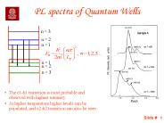
... also decreases * Nitride QW PL spectrum Electron and hole wave-functions for non-polar material Electron and hole wave-functions for polar material due ...
| PowerPoint PPT presentation | free to download

Silicon Epitaxial Wafer Market Size is forecast to reach $1.4 billion by 2026, at a CAGR of 4.8% during 2021-2026.
| PowerPoint PPT presentation | free to download
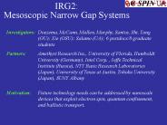
IRG2: Mesoscopic Narrow Gap Systems Investigators: Doezema, McCann, Mullen, Murphy, Santos, Shi, Yang (OU); Xie (OSU); Salamo (UA); 6 postdocs/8 graduate students
| PowerPoint PPT presentation | free to download

Beyond ferromagnetic spintronics: antiferromagnetic I-Mn-V semiconductors Tomas Jungwirth Institute of Physics in Prague & University of Nottingham
| PowerPoint PPT presentation | free to download

Title: PowerPoint Presentation Author: Solid State Last modified by: Solid State Created Date: 5/17/2002 9:03:23 PM Document presentation format: On-screen Show
| PowerPoint PPT presentation | free to download

1 Soltan Institute for Nuclear Studies, 05-400 Swierk/Otwock, Poland ... of 1 m thickness were grown on sapphire substrates using the MOVPE technique. ...
| PowerPoint PPT presentation | free to download
Laboratoire des Milieux D sordonn s et H t rog nes. Universit Pierre et ... Photolithography. Chemical etching. Si3N4 deposition. Metallic alloy deposition ...
| PowerPoint PPT presentation | free to download

1a) Phenomenology of the conventional semiconductor. valence band picture of (Ga,Mn)As ... 2a) Phenomenology of the narrow detached impurity band. pictures ...
| PowerPoint PPT presentation | free to download

Annealing studies to achieve recrystallization ... Anneal at 1000oC for 15 minutes under Ar. The Australian National University ...
| PowerPoint PPT presentation | free to view

Study of the temperature dependence of the GaN buffer layer on SiC. ... used for buffer layer deposition on sapphire, reference (a) 9000 C. 9500 C. 9700 C (~temp. ...
| PowerPoint PPT presentation | free to download

c monolithic integration of filter and detector for more compact systems. MIOMD 2005 ... Monolithically Integrated Polycrystalline PbSe Photodetectors ...
| PowerPoint PPT presentation | free to view

depends on device Area and Aspect Ratio valid only for area 2x 3x range ... of development made LDMOS offer extremely good device characteristics today ...
| PowerPoint PPT presentation | free to view

Investigation of dopant activation / extended studies. Concluding remarks ... Implanted c-axis single crystal ZnO (n-type, Cermet) with Arsenic (p-type dopant! ...
| PowerPoint PPT presentation | free to view

The existing of N interstitial compensates strain and consequently presents ... NAs substitutional and As-N split interstitial ...
| PowerPoint PPT presentation | free to view

U. Heriot-Watt. EPI Ltd. Sharp Ltd. Contents. Introduction to spin-flip Raman scattering ... Usually, the scattering (creation or annihilation) of light by ...
| PowerPoint PPT presentation | free to view

SBCT of BM-HBT was estimated to be 22% that of conventional HBT, CBC 30% of conventional HBT ... of emitter size and CBC. Schematic cross-section of device ...
| PowerPoint PPT presentation | free to download

Molecular beam epitaxy (MBE) is performed with different types of semiconducting ... Mega-Buck Evaporator. Medieval Brain Extractor. Money Buys Everything ...
| PowerPoint PPT presentation | free to view
III-IV BIPOLAR TRANSISTOR ... Increased the amount of Indium in the base of a HBT Higher electron mobility ... the electron velocity is high due ...
| PowerPoint PPT presentation | free to download

Dr' Kitt Reinhardt
| PowerPoint PPT presentation | free to view

2005 rewrite of text, based on 2004/2005 changes of cross-cuts and tables, and state-of-the-art ... ultra-high NA vector models, including polarization effects ...
| PowerPoint PPT presentation | free to view

... substrate and manifest a fascinating fine structure in their local vibrational ... frequency of the LVM and its fine structure components are demonstrated to be ...
| PowerPoint PPT presentation | free to download

Nanoscale Analytics
| PowerPoint PPT presentation | free to view

... available 4H-SiC wafers grown by the PVT technique with an 8 off-cut angle ... Scratches parallel to the off-cut direction create half-loops whose surface ...
| PowerPoint PPT presentation | free to view

Soon-Yong Kwon, Seong-Il Baik, Hee Jin Kim, Young-Woon Kim, Jung-Won Yoon ... According to Matthews and Blakeslee's formula, the critical thickness for ...
| PowerPoint PPT presentation | free to view

... contained all the colors of the rainbow, with wavelengths from about 390 nm to 780 nm. He actually labeled this rainbow a 'spectrum' ...
| PowerPoint PPT presentation | free to view
Anneal sample as before (1600 for 30 min) Remove Carbon Cap (RIE with O2) ... Channel mobility: 40- 45 cm2/Vs (on epilayer layer annealed at 1600 C) Stable up to 15V ...
| PowerPoint PPT presentation | free to download

Title: Presentazione di PowerPoint Author: SilviaR Last modified by: silvia Created Date: 5/30/2005 8:19:12 AM Document presentation format: On-screen Show
| PowerPoint PPT presentation | free to view

with single bunch crossing tagging Chronopixel Sensors for the ILC J. E. Brau, N. B. Sinev, D. M. Strom University of Oregon, Eugene C. Baltay, H. Neal, D. Rabinowitz
| PowerPoint PPT presentation | free to download

Mechanical behaviour of a- and c- axis epitaxial ZnO grown on sapphire ... is inhibited by the underlying sapphire substrate for a-axis layers, but not for ...
| PowerPoint PPT presentation | free to view

LED design has evolved to increase extraction efficiency, but all forms have the same basic epilayer structure (a). Metallic contacts can be added to this structure ...
| PowerPoint PPT presentation | free to view

Title: Presentazione di PowerPoint Author: Lab S. E. Last modified by: Valerio Re Created Date: 3/12/2003 1:56:02 PM Document presentation format
| PowerPoint PPT presentation | free to download

Simulations suggest that 3 s shaping time allows ladders to be read from end only ... Response to signals between and 128 mips (in factor-of-two octaves) ...
| PowerPoint PPT presentation | free to view
In-situ Iridium Refractory Ohmic Contacts to p-InGaAs Ashish Baraskar, Vibhor Jain, Evan Lobisser, Brian Thibeault, Arthur Gossard, Mark J. W. Rodwell
| PowerPoint PPT presentation | free to download

Semiconductor Spintronics: What s It All About? Bruce D. McCombe Department of Physics and Center for Advanced Photonic and Electronic Materials
| PowerPoint PPT presentation | free to view

To Get More Details @ http://www.bigmarketresearch.com/global-super-junction-mosfet-2014-2018-market “Big Market Research : Global Super Junction MOSFET Market - Size, Share, Trends, Analysis, Research, Report and Forecast, 2014-2018” Super junction MOSFETs are power semiconductor components used for high-frequency and high-voltage applications. They are fabricated using two types of technology, multi-epitaxial growth and deep trench. Multi-epitaxial growth technology uses the multiple epitaxy and doping processes to create a doped area in the epilayer, which diffuses and creates an N-doped layer. Deep trench technology uses the deep reactive ion etching technique to create a trench, which is then filled with an N-doped material to form the super junction structure.
| PowerPoint PPT presentation | free to download

Mechanical strainstress characterization techniques in epitaxial layers
| PowerPoint PPT presentation | free to view

Univ. of Napoli, Italy. 3 Cambridge Semiconductor (CamSemi), UK. EU research program ROBUSPIC ... NAPOLI. UNIVERSITY. Differences with Vertical IGBT (1) ...
| PowerPoint PPT presentation | free to view

NAPOLI. UNIVERSITY ... Univ. of Napoli, Italy. 3 Cambridge Semiconductor (CamSemi), UK. EU research program ROBUSPIC ... NAPOLI. UNIVERSITY. IGBT models not ...
| PowerPoint PPT presentation | free to view

The approach can be implemented 'ab-initio' where the orbitals are the basis ... are necessary due to the band gap problem of ab-initio approaches ...
| PowerPoint PPT presentation | free to view

Next Generation Electronics from Silicon Carbide to Carbon Nanotubes and Smart Sensors: Paradigms for UMD-ARO/ARL Collaboration Neil Goldsman Dept. of Electrical and ...
| PowerPoint PPT presentation | free to download

with similar edges and angle, that are first positioned over one ... which is a widespread twin by reticular merohedry (index 1 with zero obliquity) of diamond ...
| PowerPoint PPT presentation | free to view

Title: Presentazione di PowerPoint Author: Lab S. E. Last modified by: Valerio Re Created Date: 3/12/2003 1:56:02 PM Document presentation format
| PowerPoint PPT presentation | free to download

US Office of Naval Research. US Army Aviation and Missiles Command ... engineering (% of Ge, grading) and selective placement ...
| PowerPoint PPT presentation | free to view

Some examples about the correlation of micro-PL measurements with the ... 2) energies of the phon- ons. 3) overall crystal quality. 4) presence of impurities ...
| PowerPoint PPT presentation | free to view

Chemistry of Epitaxy Polysilicon layers may be formed by CVD Sources :Solid State Electronic Devices B. Streetman and S. Banerjee Prentice Hall 2005 (6th Edition ...
| PowerPoint PPT presentation | free to view

A Level-Set Method for Modeling Epitaxial Growth and Self ... B. Lita et al. (Goldman group), APL 74, 2824 (1999) Islands nucleate 'on top' of lower islands ...
| PowerPoint PPT presentation | free to view

INTRODUCTION The Group III Nitrides are of continuing interest due to their application in blue/UV optoelectronic and high power, ...
| PowerPoint PPT presentation | free to download

In2O3/Ga2O3 + 4H 2H2O + In2O/Ga2O In2O3/Ga2O3 + 4H H2O + 2InOH/2GaOH Similarly carbon containing complexes (InGaAs-C) are broken into volatile products GHz 1400 ...
| PowerPoint PPT presentation | free to download

Novel SiGe Semiconductor Devices for Cryogenic Power Electronics ICMC/CEC August-September 2005 Keystone, Colorado Authors Goals Develop SiGe devices for cryogenic ...
| PowerPoint PPT presentation | free to view