Prototype LNA - PowerPoint PPT Presentation
1 / 9
Title:
Prototype LNA
Description:
1 mW through source follower. 1 mW through biasing ... 6 dB is lost through source follower. 2nd generation uses integrated capacitive transformer ... – PowerPoint PPT presentation
Number of Views:45
Avg rating:3.0/5.0
Title: Prototype LNA
1
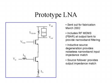
Prototype LNA
- Sent out for fabrication March 2002
- Includes RF MEMS (FBAR) at output tank to
provide narrowband filtering - Inductive source degeneration provides noiseless
narrowband input impedance match - Source follower provides output impedance match
Vdd
Lchoke
FBAR
Vout
Vbias
Lg
Vin
Ls
2
(No Transcript)
3
Measured S Parameters
4
Measurement versus Simulation
- Measured (_at_ 1.89 GHz)
- S11 -13.44 dB
- S21 6.77 dB
- S12 -24.4 dB
- S22 -7.35 dB
- Simulation
- S11 -10.73 dB
- S21 12.61 dB
- S12 -47.58 dB
- S22 -11.81 dB
5
Performance Summary
- Power 3 mW total (from 1 V source)
- 1 mW through LNA
- 1 mW through source follower
- 1 mW through biasing
- 1 dB Compression Point -18.5 dBm (simulation
-19.6 dBm) - Power Gain 6.77 dB
- Bandwidth 4 MHz centered at 1.89 GHz
- Noise Figure to be measured (simulation
3.5 dB)
6
What was learned
- LNA results are close to simulation
- Forward gain is degraded by capacitive parasitics
from board. - Q of FBAR is decreased significantly
- 2nd generation integrates all sensitive nodes on
chip - 6 dB is lost through source follower
- 2nd generation uses integrated capacitive
transformer - On-chip gate inductor contributes noise and
degrades forward gain - Accurate modeling of transistors and parastics is
absolutely necessary - Lower power can be achieved by decreasing current
through bias transistors, as well as using a
passive output impedance matching network.
7
2nd Prototype LNA
NO FBAR NARROWBAND FILTERING IN SECOND STAGE
RF OUT
NO SOURCE DEGENERATION, INPUT MATCH BY NQS GATE
RESISTANCE
RF IN
INPUT IMPEDANCE MATCHING
shematic of LNA in receiver chain. The output
impedance matching network is not shown.
8
Simulated S Parameter Plots
S11
S21
16 dB
-39 dB
9
Simulated Performance Summary
- S21 16 dB
- S11 -39 dB
- AV 30 dB
- Bias Current 1.5 mA
- Power 1.8 mW
- Noise Figure 2.6 dB
- Linearity (IP3) -17.3 dBm


