Miss Penalty Reduction Techniques (Sec. 5.4) - PowerPoint PPT Presentation
1 / 10
Title:
Miss Penalty Reduction Techniques (Sec. 5.4)
Description:
Local miss rate: ... Miss Penalty Reduction Techniques (Cont'd) ... Miss penaltyL2 = 50 CC. What's the impact of L2 cache associativity on the miss penalty? ... – PowerPoint PPT presentation
Number of Views:31
Avg rating:3.0/5.0
Title: Miss Penalty Reduction Techniques (Sec. 5.4)
1
Miss Penalty Reduction Techniques (Sec. 5.4)
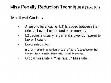
- Multilevel Caches
- A second level cache (L2) is added between the
original Level-1 cache and main memory. - L2 cache is usually larger and slower compared to
Level-1 cache - Local miss rate
- (no. of misses in a particular cache / no. of
accesses to that cache) for example, Miss
rateL1 and Miss rateL2 - Global miss rate Miss rateL1 Miss rateL2
2
Miss Penalty Reduction Techniques (Sec. 5.4)
- Multilevel Caches (contd.)
- 1000 mem references,40 misses in L1 cache20
misses in L2 cacheCompute various miss rates. - Miss rate L1 40/1000 4
- Miss rate L2 20/40 50Global Miss rate 4
x 50 2 - Ave Mem Access time Hit timeL1 Miss rateL1 x
Miss PenaltyL1 - Miss PenaltyL1 Hit timeL2 Miss rateL2 x Miss
PenaltyL2
3
Miss Penalty Reduction Techniques (Contd)
Example on Page 420 2-way set associative
increases hit time by 0.1 CC Hit timeL2 for
direct mapped 10 CC Local Miss rateL2 for
direct mapped 25 Local Miss rateL2 for 2-way
set associative 20 Miss penaltyL2 50
CC Whats the impact of L2 cache associativity on
the miss penalty? Miss penalty 1-wayL1
10(0.25x50) 22.5 CC Miss Penalty 2-wayL1
10.1 (0.20 x50) 20.1CC
4
Miss Penalty Reduction Techniques (Contd)
- Early Restart and Critical Word First
- Early Restart Send to CPU the requested word as
soon as it arrives - Critical Word First Get the requested word from
the memory first, send it to the CPU and then
load the block in the cache - Giving Priority to Read Misses Over Write
- Serve reads before completing the writes
- In write-through cache, write buffers complicate
memory accesses they may hold a location needed
on a read miss. - Wait on a read miss until the write buffer is
empty, or - Check the contents of the write buffer and
continue - Merging Write Buffers
- This technique was covered in Sec. 5.2, Fig 5.6.
5
Hit Time Reduction Techniques (Sec. 5.5)
- Small and Simple Cache
- Small caches can fit on the same chip as the
processor - Simple caches such as direct-mapped caches have
low hit time - Some L2 cache designs keep the tags on chip and
the data off chip
6
Hit Time Reduction Techniques (Contd)
- Avoiding Address Translation During Indexing of
the Cache - Virtual caches use virtual addresses for the
cache, instead of physical addresses - Virtual addressing eliminates address translation
time from a cache hit - Virtual caches have several issues
- Protection is checked during virtual to physical
address translation - Whenever a process is switched, virtual addresses
refer to different physical addresses - Multiple virtual addresses for the same physical
address could result in duplicate copies of the
same data in a virtual cache - A compromise is a virtually indexed but
physically tagged cache.
7
Hit Time Reduction Techniques (Contd)
- Pipelined Cache Access
- Tag and data portions are split, so they can be
addressed independently - Data from the previous write is written while tag
comparison is done for the current write - Thus writes can be performed back to back at one
per clock cycle
8
Main Memory and its Organization (Sec. 5.6)
- Main memory is the next lower level memory after
cache - Main memory serves the demands of a cache as well
as the I/O interface - Memory bandwidth is the number of bytes read or
written per unit time - Assume a basic memory organization as follows
- 4 CC to send an address
- 24 CC for the access time per word
- 4 CC to send a word of data
- A word is 4 byte
- A cache block is 4 words
- Miss Penalty 4 x (4 244) 128 CC
- Band width 16/128 1/8 byte per CC
9
Achieving Higher Memory Bandwidth
- Wider Main Memory
- Increase the width of the cache and the main
memory (Figure 5.31 b) - If the main memory width is doubled, the miss
penalty will be 2 x ( 4244) 64CC, and the
bandwidth will be 16/64 ¼ byte per CC - There is added cost of a wider bus and a
multiplexer between the cache and the CPU - The multiplexer may be on the critical timing
path - A second level cache helps, as the multiplexer
comes between level 1 and level 2 caches - Another drawback is that minimum increments are
doubled or quadrupled - There are some issues with error correction that
complicate the design further
10
Achieving Higher Memory Bandwidth (Contd)
- Simple Interleaved Memory
- Memory chips are organized in banks to read or
write multiple words at a time - The banks are often one word wide (Figure 5.32)
- The miss penalty in our ongoing example, with
four banks is 4244x4 44CC, and the bandwidth
will be 16/44 0.36 byte per CC - Power vs. performance trade off
- Independent Memory Banks
- A generalization of interleaving
- Allows multiple independent accesses, with
independent memory controllers, and separate
address and data lines - Used in an environment where several devices,
such as I/O devices and multiple processors,
share the memory bandwidth.


