Diapositive 1 - PowerPoint PPT Presentation
1 / 9
Title:
Diapositive 1
Description:
Objective: comparison of the different processes and equipments of hot embossing ... Quartz molds for UV-NIL: E-Beam lithography on 100 mm quartz wafers ... – PowerPoint PPT presentation
Number of Views:32
Avg rating:3.0/5.0
Title: Diapositive 1
1
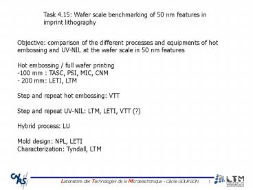
Task 4.15 Wafer scale benchmarking of 50 nm
features in imprint lithography
- Objective comparison of the different processes
and equipments of hot embossing and UV-NIL at the
wafer scale in 50 nm features - Hot embossing / full wafer printing
- 100 mm TASC, PSI, MIC, CNM
- 200 mm LETI, LTM
- Step and repeat hot embossing VTT
- Step and repeat UV-NIL LTM, LETI, VTT (?)
- Hybrid process LU
- Mold design NPL, LETI
- Characterization Tyndall, LTM
2
Planning
- Deliverable D4.21 at M36 March 2007
- Delivery of the molds during the Glasgow meeting
September 11th - Imprint processes until end of October
- November 1st wafers sent to Tyndall and LTM for
characterization - November and December characterization, and
eventually new imprints if needed - January characterization of the new imprints
- February redaction of the deliverable
Mold fabrication
Imprint 1
Redaction
Characterization Imprint 2
Characterization
3
Mold fabrication in LETI
- Si wafers 100mm (and 200 mm for LTM-LETI)
- E-beam lithography in NEB22 resist
- thickness after development 100 nm for 50 nm
resolution - Etching on LAM equipment in LTM
- etching depth 100 nm (limited by the small
resist budget) - Wet deposition of the anti-sticking layer
Optool - Quartz molds for UV-NIL E-Beam lithography on
100 mm quartz wafers - Resolution we will try to achieve 50/50 but with
no guarantee - 50/100 nm already achieved
- VTT what is the mold size and thickness for the
stepper? - LU What molds do you need?
- The molds will be given back to LETI after the
benchmarking
4
NIL process Hot embossing
- PSI Jenoptik HEX03 TASC Weber press
- MIC EVG520HE (100mm) LETI/LTM EVG520HE (200mm)
- CNM Obducat VTT step and repeat on NPS200
- LU Obducat (process has to be precised)
- Imprints 1
- - Two wafers with the best process achievable
each partner chooses the resist, its thickness
and the process parameters, but the rule is to
try to minimize the residual thickness - Two wafers with the mr-I7010 using a 100 nm film
- Imprints 2 depending on the characterization
results
5
NIL process UV-NIL
- LTM imprints on the EVG NIL-Stepper (the
installation is just finishing) - Material NILTM105 or AMONIL
- VTT which materials do you use?
6
Mold layout
Limitation exposure time since LETI has to
produce 5 100mm molds and 1 200mm mold, but it is
important that all the molds are fabricated in
the same place with the same process
1 mm² lines 50/50 nm
Line gratings with various densities 100/100,
100/200, 100/500 Surface1mm x 200µm for each
grating
T- Lines 100/100 Line length 500 µm 50 periods
Pb charac Tyndall 3x1 mm Or 0.5x1.5 mm
Mold depth 100nm
7
Characterization Tyndall and LTM
- Scatterometry
- LTM ellipsometer spot size 20µm, but only for
non contaminated wafers only for the 200 mm
wafers - We have also a ellipsometer for contaminated
wafers, but the spot size is 2x2mm - Tyndall ellipsometer spot size 1x3 mm but could
be reduced to 0.5x1.5mm - If the grating area is large enough, the spectra
will be recorded in Tyndall and LTM will help for
the fit and analysis. - Problem 0.5x1.5mm spot size printed grating
1x2 mm !! - Is it achievable by LETI? If yes, only for one
structure size. Is 1x2mm large enough to get rid
of the border effect? - Conclusion is there someone having an
ellipsometer with a smaller spot size? - MEB will be very useful but not for all the
materials for example, it is very difficult to
measure precisely the residual thickness in
mr-I7010 for charging reasons.
8
Scatterometry
CD, hi and hr measured in 50 nm lines Error
parameter to indicate if the fit is good
enough Error gt 1 non uniform hi or hr
Morphology we can characterize the slope in case
in case of non vertical lines, but the
calculation is longer / no information on the
roughness
9
summary
- If we are able to produce the molds for the next
NAPA meeting, and if everybody is able to respect
the planning, we should have nice results for
next march!!


