Boron etch stop process - PowerPoint PPT Presentation
1 / 8
Title:
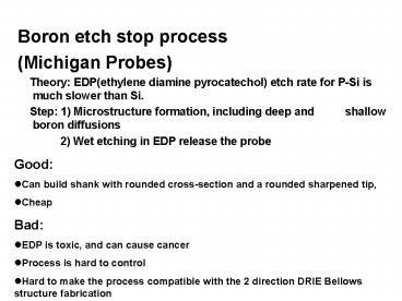
Boron etch stop process
Description:
Boron etch stop process (Michigan Probes) Theory: EDP(ethylene diamine ... Step: 1) Microstructure formation, including deep and shallow boron diffusions ... – PowerPoint PPT presentation
Number of Views:226
Avg rating:3.0/5.0
Title: Boron etch stop process
1
- Boron etch stop process
- (Michigan Probes)
- Theory EDP(ethylene diamine pyrocatechol)
etch rate for P-Si is much slower than Si. - Step 1) Microstructure formation, including
deep and shallow boron diffusions - 2) Wet etching in EDP release the
probe
- Good
- Can build shank with rounded cross-section and a
rounded sharpened tip, - Cheap
- Bad
- EDP is toxic, and can cause cancer
- Process is hard to control
- Hard to make the process compatible with the 2
direction DRIE Bellows structure fabrication
2
- SOI (Silicon on Insulator) Wafer technology
(Stanford, Berkeley, Sweden) - Theory Plasma etching rate for SiO2 is much
slower than Si. - Step 1) SOI wafers with different silicon layer
thickness are commercial available - 2) Front side DRIE to define the probes
- 3) Back side DRIE to release the probes
- Bad
- Expensive
- Probe shank are in the same thickness
- Good
- Process is easy to control
- process is compatible with the 2 direction DRIE
Bellows structure fabrication
3
16-site Neural Probe Design
Trace width 5?m Site size 10 ?m 10 ?m
4
Process Flow
- SOI wafer
- Coat parylene as an insulating layer, deposit and
pattern (lift off) Ti/Au as the electrode traces
and the bonding pads - Coat and pattern (plasma etch) parylene to open
the electrode sites and the bonding pads - Deposit and pattern (lift off) Ti/Pt as the
electrode sites - Deposit parylene as a protective layer and
pattern it - Font side silicon etch
- Back side silicon etch
- Oxide etch and resist strip
5
Connection
Standard Bus Interface
PCB
Bonding Pads for Gold Wire Bonding
Silicon Chip
6
Parylene Flexible Cable
7
Power Interface
Power Management
RAM
MUX
ADC
AMP
Bus Interface
RPROM
Wireless Interface
IC
IC
IC
IC
8
Probe Array


