PowerPointPrsentation - PowerPoint PPT Presentation
1 / 1
Title:
PowerPointPrsentation
Description:
Nano-particles have specific chemical and electrical properties. ... Skimmer. Deflection. capacitor. Repelling. potentials. Faraday cup. Current amplifier ... – PowerPoint PPT presentation
Number of Views:74
Avg rating:3.0/5.0
Title: PowerPointPrsentation
1
Cluster-jet addressing of nano-particles to
provide functional structures
J. Meijer1, T. Vogel1, D. Reuter1, I. Rangelow2,
H. Wiggers3 1Ruhr-Universität Bochum,
2GH-Universität Kassel, 3Universität
Duisburg/Essen
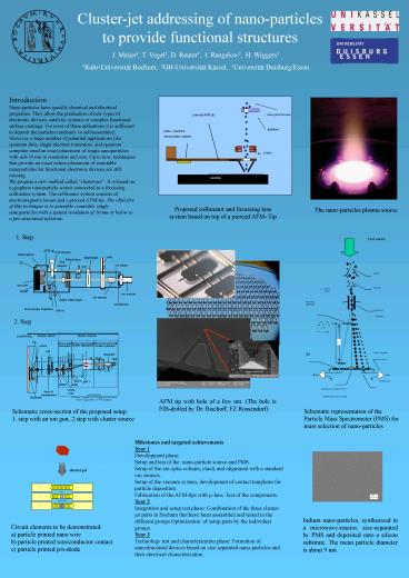
Introduction Nano-particles have specific
chemical and electrical properties. They allow
the production of new types of electronic
devices, catalytic systems or complex functional
surface coatings. For most of these aplications
it is sufficient to deposit the particles
randomly or self-assembled. However, a large
number of potential applications like quantum
dots, single electron transistors, and quantum
computer need an exact placement of single
nanoparticles with sub-10 nm in resolution and
size. Up to now, techniques that provide an exact
online-placement of countable nanoparticles for
functional electronic devices are still
missing. We propose a new method called
cluster-jet. It is based on a gasphase
nanoparticle source connected to a focussing
collimator system. The collimator system consists
of electromagnetic lenses and a pierced AFM-tip.
The objective of this technique is to assemble
countable single nanoparticles with a spatial
resolution of 10 nm or below to a pre-structured
substrate.
nano-particle beam
Proposed collimator and focussing lens system
based on top of a pierced AFM- Tip
The nano-particles plasma source
1. Step
2. Step
AFM tip with hole of a few nm. (The hole is
FIB-drilled by Dr. Bischoff, FZ Rossendorf)
Schematic representation of the Particle Mass
Spectrometer (PMS) for mass selection of
nano-particles
Schematic cross-section of the proposed setup 1.
step with an ion gun, 2.step with cluster source
Milestones and targeted achievements Year 1
Development phase Setup and test of the
nano-particle source and PMS. Setup of the ion
optic column, check and alignment with a standard
ion sources. Setup of the vacuum system,
development of contact templates for particle
deposition. Fabrication of the AFM-tips with
µ-lens. Test of the components. Year
2 Integration and setup test phase Combination
of the three cluster-jet parts in Bochum that
have been assembled and tested in the different
groups Optimization of setup parts by the
individual groups. Year 3 Technology test and
characterization phase Formation of
nanostructured devices based on size separated
nano-particles and their electrical
characterization.
cluster jet
Indium nano-particles, synthesized in a
microwave-reactor, size-separated by PMS and
deposited onto a silicon substrate. The mean
particle diameter is about 9 nm.
- Circuit elements to be demonstrated
- particle printed nano wire
- b) particle printed semiconductor contact
- c) particle printed p/n-diode


