
Electrodeposit PowerPoint PPT Presentations
All Time
Recommended

Download free PDF Sample: https://bit.ly/3iccEJh #ElectrodepositedCopperFoils #MarketAnalysis Electrodeposited Copper Foils market is segmented by Type, and by Application. Players, stakeholders, and other participants in the global Electrodeposited Copper Foils market will be able to gain the upper hand as they use the report as a powerful resource.
| PowerPoint PPT presentation | free to download

Hence, quantitative analysis of crack size and distribution is so important, ... The micro-size crack seems to be 'Calabash shape' which is formed by the ...
| PowerPoint PPT presentation | free to view

Multilayer structures are most commonly prepare by vacuum based ... (this texture proved to be superior to the (110) and (111) textures for the GMR effect) ...
| PowerPoint PPT presentation | free to view

TBRC global copper foil market report includes rolled copper foil, electrodeposited copper foil, printed circuit boards, batteries, electromagnetic shielding
| PowerPoint PPT presentation | free to download

... as on Tues. Mix 50 ml IrOx with 1 ml phage. Electrodeposit 10 minutes 7.5V. Mix sample. Electrodeposit 10-20 minutes more. Should see purple pattern ...
| PowerPoint PPT presentation | free to download

As a component of etch resists in the PCB fabrication process ... Hexavalent chromium is used to passivate the surfaces of zinc and zinc alloy electrodeposits ...
| PowerPoint PPT presentation | free to view

1 mm. Silica structures. Electrodeposited metal particles coating carbon nanotubes ... was introduced in the 'Advanced Characterization Methods' (Phys 502) class. ...
| PowerPoint PPT presentation | free to view

... is the process in which nanoparticles are adsorbed and plated into a metal film. The growth of an electrodeposited film along the electrode is controlled by the ...
| PowerPoint PPT presentation | free to view

... is the process in which nanoparticles are absorbed and plated into a metal film. The growth of an electrodeposited film along the electrode is controlled by the ...
| PowerPoint PPT presentation | free to view

... curves for electrodeposited nickel (a), aluminium alloy 1420-Al processed by ... contributes to plastic flow of coarse-grained polycrystalline aluminium. ...
| PowerPoint PPT presentation | free to view

With the use of a rigid flex PCB(rigid FPC), flexible circuit substrates and rigid circuit substrates are covered together. Rigid-flex PCBs cross the limits of conventional rigid PCBs and the one of a kind properties of flex circuits that utilization high-flexibility electrodeposited or moved strengthened copper conductors photograph carved onto a flexible protecting film. Flex circuits incorporate stack-ups produced using a flexible polyimide, for example, Kapton or Norton and copper-covered together through warmth, acrylic cement, and weight.
| PowerPoint PPT presentation | free to download

The Copper Foils for Lithium Ion Batteries market is analysed and market size information is provided by regions (countries).
| PowerPoint PPT presentation | free to download

According to the latest research report by IMARC Group, The global copper foil market size reached US$ 5.7 Billion in 2022. Looking forward, IMARC Group expects the market to reach US$ 8.7 Billion by 2028, exhibiting a growth rate (CAGR) of 7% during 2023-2028. More Info:- https://www.imarcgroup.com/copper-foil-market
| PowerPoint PPT presentation | free to download

Electro-Deposited (ED) Copper Foil market is segmented by region (country), players, by Type, and by Application.
| PowerPoint PPT presentation | free to download

M ssbauer study of swift heavy ion irradiated Fe-Ni-Cr multilayers ... in vacuum deposited FeNiCr multilayers due to swift heavy ion irradiation, Nucl. ...
| PowerPoint PPT presentation | free to download
Storage and aging of a-C: air vs N2 for samples from MBB#2 magnet ... In planar magnetron configuration, at room temperature. Aim: more sp2 ...
| PowerPoint PPT presentation | free to download

Philips Thru Via Imaging Philips Thru Via Imaging Quadruple leads in a single through-wafer hole and a toroid structure Exposure Using Phase Gratings Schematic ...
| PowerPoint PPT presentation | free to download

IC soldered to printed circuit board. Looked at pre-configured modules in COMSOL ... IC soldered to printed circuit board. Future Work ...
| PowerPoint PPT presentation | free to view
The global copper foil market is primarily driven by the escalating demand for PCBs in consumer electronics such as laptops, smartphones and tablets. Additionally, the increasing adoption of electric vehicles (EVs) due to the growing environmental concerns and rising greenhouse gas (GHG) emissions has augmented the product demand Ask Analyst for Customization and Explore Full Report with TOC & List of Figure: Visit the following link: https://www.imarcgroup.com/copper-foil-market E-mail: sales@imarcgroup.com Contact: +91-120-415-5099
| PowerPoint PPT presentation | free to download

The global copper foil market is primarily driven by the escalating demand for PCBs in consumer electronics such as laptops, smartphones and tablets. Additionally, the increasing adoption of electric vehicles (EVs) due to the growing environmental concerns and rising greenhouse gas (GHG) emissions has augmented the product demand Get a PDF Sample for more detailed market insights: Visit the following link: https://www.imarcgroup.com/copper-foil-market E-mail: sales@imarcgroup.com Contact: +91-120-415-5099
| PowerPoint PPT presentation | free to download

horizontal electrode, faced upward and downward vertical magnetic field, dB/dt ... vertical copper electrode % Fe = 35 ... Create an anisotropy on electrode ...
| PowerPoint PPT presentation | free to view

INTRODUCTION It is known that the high-powerful electromagnetic fields cause ... Vuchkov,L., Nanoscience&Nanotechnology, 3, pp. 145-147, Heron Press, Sofia, 2003 ...
| PowerPoint PPT presentation | free to view

... copper equivalent to those of wrought nickel have been demonstrated (a 50 ... Elevated temperature ductility of electroformed copper to 500 F has been ...
| PowerPoint PPT presentation | free to download

... Tube Regen Chamber Electroformed using new High Strength Materials ... NASA Tech Brief articles of the new materials have been written and approved for ...
| PowerPoint PPT presentation | free to download

Equipment/installation. Basic requirements are a coating bath, ... Hardness and wear resistance can now be comparable with brass and aluminium by using nanocomposite ...
| PowerPoint PPT presentation | free to download

1- BMR over 3000% in Ni nanocontact at room temperature (PRB 66, 2002) 2- 100,000 % BMR in stable Ni nanocontacts at room temperature (PRB, 67,2003) ...
| PowerPoint PPT presentation | free to view

Nanofabrication and Characterization of nanosturcture Device ... Richard D. Piner, Jin Zhu, Feng Xu, Seunghun Hong, Chad A. Mirkin, Science, 283, 5402 (1999) ...
| PowerPoint PPT presentation | free to view

FABRICATION DES CIRCUITS IMPRIMES I Le Produit PRINTED CIRCUIT BOARD FABRICATION I Product overview Le Produit Products Overview Historique Fonction d un CI Les ...
| PowerPoint PPT presentation | free to download
FABRICATION DES CIRCUITS IMPRIMES II Mat riaux de base PRINTED CIRCUIT BOARD FABRICATION II Base Materials La fabrication des circuits imprim s
| PowerPoint PPT presentation | free to download

NER: Nano-Biodevices For Reliable Long-Term Recording and Stimulation of Neuronal Activity ... B) Close-up of white box in (A) showing vertically arranged single gold ...
| PowerPoint PPT presentation | free to download
Lecture 24: Strengthening and Recrystallization PHYS 430/603 material Laszlo Takacs UMBC Department of Physics How can we make a material strong - have large yield ...
| PowerPoint PPT presentation | free to download

Producing Synthetic Diesel from Natural Gas and Carbon Dioxide Using Nano-Structured Catalyst Dr. Chester Wilson Institute for Micromanufacturing
| PowerPoint PPT presentation | free to view

Influence of static magnetic fields in nickel electrodeposition Adriana Ispas, Andreas Bund, Waldfried Plieth SFB 609 Outline Electrochemical Quartz Crystal ...
| PowerPoint PPT presentation | free to download

FABRICATION DES CIRCUITS IMPRIMES II Mat riaux de base PRINTED CIRCUIT BOARD FABRICATION II Base Materials Mat riaux de base Base materials Stratifi s rigides ...
| PowerPoint PPT presentation | free to download

Metallization of insulators (plastics) using polypyrrole as precoat D. Yfantis, N. Vourdas, A. Yfantis, S. Kakos, A. Katsori, N. Yfantis, D. Schmeisser
| PowerPoint PPT presentation | free to download

1940 : Invention aux USA pour des applications militaires (missiles) ... Alliage refondu Alloy reflow. Alliage. Vernis pargne. Solder mask. La fabrication des ...
| PowerPoint PPT presentation | free to view

1 -ray production by the reactions Li(p, )Be and B(p, )C tested at the ... Targets deposited on polished copper discs. Thermal evaporation. Lithium Fluoride ...
| PowerPoint PPT presentation | free to view

SYNTHESIS OF COPPER NANOWIRES WITH NANO-TWIN SUBSTRUCTURES 1Joon-Bok Lee 2Dr. Bongyoung I. Yoo 2Dr. Nosang V. Myung 1Department of Chemical Engineering, A-217 ...
| PowerPoint PPT presentation | free to view

About Omics Group OMICS Group International through its Open Access Initiative is committed to make genuine and reliable contributions to the scientific community.
| PowerPoint PPT presentation | free to view

The BMR curves of iron and permalloy contacts on Cu film respectively. ... In the case of permalloy, the right one, we measured the sample two time, each ...
| PowerPoint PPT presentation | free to view

chamber is 0.6 m in height and 1.5 in diameter. vacuum inside is around ... the University of California (UCLA) have demonstrated a memory cell which can be ...
| PowerPoint PPT presentation | free to download

Advanced Magnets and Implications for BPX-I. MIT Plasma Science and Fusion Center ... 2) Active clamping. 3) Recool to 30 K. MIT Plasma Science and Fusion Center ...
| PowerPoint PPT presentation | free to download

Lecture 25: The Liquid State Nucleation and Metallic Glasses PHYS 430/603 material Laszlo Takacs UMBC Department of Physics
| PowerPoint PPT presentation | free to download

Shape Anisotropy Crystalline Anisotropy. Magnetic property of ... Perpendicular magnetic anisotropy to substrate. Hc vs magnetization angle. VSM measurement ...
| PowerPoint PPT presentation | free to view

Electrochemistry in Nanoelectronics
| PowerPoint PPT presentation | free to view

Investigation of Hydrogen Adsorption and Absorption in Palladium thin films, J. Electrochem. ... Absorption current swallows adsorption current. 10 ML Pd Film ...
| PowerPoint PPT presentation | free to view

Title: PowerPoint-Pr sentation Author: Szot Last modified by: hutchby Created Date: 6/27/2003 9:17:55 PM Document presentation format: On-screen Show
| PowerPoint PPT presentation | free to view
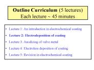
Outline Curriculum (5 lectures) Each lecture 45 minutes Lecture 1: An introduction in electrochemical coating Lecture 2: Electrodeposition of coating
| PowerPoint PPT presentation | free to download

Micrograph of a Utah Electrode Array (UEA) with 100 equal length probes. ... Optical micrographs of initial Au coil samples on polyimide substrates with a ...
| PowerPoint PPT presentation | free to view
1) Alpha sources spots on wires. Sorces at different ... sinter gl. 45. Results: FairChild. 68 75. 5 Hz. 75 75. 200 Hz (75//75)x2. 3 Hz. February 9th 2005 ...
| PowerPoint PPT presentation | free to download

Adhesion and Etching of Nickel-Chromium Tiecoat on Adhesiveless Flexible Laminate by Bergstresser, T., Hilburn, R. and Wang, J. Gould Electronics
| PowerPoint PPT presentation | free to view

X-ray Diffraction: Principles and Practice Ashish Garg and Nilesh Gurao Department of Materials Science and Engineering Indian Institute of Technology Kanpur
| PowerPoint PPT presentation | free to download

Microbial infections in oral cavity Wenyuan Shi
| PowerPoint PPT presentation | free to view

10th International Conference on Calorimetry in High Energy Physics Calor 2002. ... Any electronegative molecule (O2 ) absorbs electrons and decreases. the signal. ...
| PowerPoint PPT presentation | free to download

10th International Conference on Calorimetry in High Energy ... Energy deposited over ~ 20 m constant currant. Ramping on the electric field E (~20 values) ...
| PowerPoint PPT presentation | free to view