
Characteristics Of A Diode PowerPoint PPT Presentations
All Time
Recommended

Chapter 10 Diodes 1. Understand diode operation and select diodes for various applications. 2. Analyze nonlinear circuits using the graphical load-line technique.
| PowerPoint PPT presentation | free to view

Clipper circuits that serve to protect circuits from damage as a result of over ... Clippers are common in computer circuits. Chapter 9 - Diodes and Diode Circuits. 19 ...
| PowerPoint PPT presentation | free to view

A varactor diode is also called varicap diode. Lets look into the construction, working of diode, characteristics and applications of varactor diode
| PowerPoint PPT presentation | free to download

Schottky diode I-V characteristics Schottky diode is a metal-semiconductor (MS) diode Historically, Schottky diodes are the oldest diodes MS diode electrostatics and ...
| PowerPoint PPT presentation | free to download

In this case, drift current is limited NOT by HOW FAST carriers are swept across ... To a first approximation, the drift current does not change with the ...
| PowerPoint PPT presentation | free to view

Chapter 9. PN-junction diodes: Applications Diode applications: Rectifiers Switching diodes Zener diodes Varactor diodes (Varactor = Variable reactance)
| PowerPoint PPT presentation | free to view

Chapter 6-1. PN-junction diode: I-V characteristics Topics: PN Junction under bias (qualitative discussion) Ideal diode equation Deviations from the ideal diode
| PowerPoint PPT presentation | free to view

InAs Quantum Dot Laser Diodes: Structure, Characteristics, Temperature ... readouts of thermocouple and pyrometer were calibrated using 2x2 2x4 transition ...
| PowerPoint PPT presentation | free to view

Title: Slide 1 Author: Ray Teng Last modified by: BCC Created Date: 9/23/2003 6:12:31 PM Document presentation format: Custom Company: UR-PAS Other titles
| PowerPoint PPT presentation | free to download

... contacts of the diode are distances Wp from the junction on the p ... Avalanche breakdown in a diode is modeled by the equation (n is a model parameter) ...
| PowerPoint PPT presentation | free to view

Given a half-wave rectifier with: VS = 20Vp-p ... (controlled breakdown). Otherwise, ... (PIV) IS For Silicon diodes, ...
| PowerPoint PPT presentation | free to view

Chapter 6. pn Junction Diode: I-V Characteristics pn Junction I-V Characteristics Electron Drift Flow Electron Diffusion Flow Electron Diffusion Flow Electron Drift ...
| PowerPoint PPT presentation | free to view
In this presentation PN junction in thermal equilibrium is discussed. Depletion width, charge density, Electric field and potential is explained
| PowerPoint PPT presentation | free to download

The attached narrated power point presentation attempts to explore the construction and working principle of PN Junction Diodes.
| PowerPoint PPT presentation | free to download

Schottky diode is also known as barrier diode. Learn more about Schottky diode working, construction, V-I characteristics, features and applications
| PowerPoint PPT presentation | free to download

In this presentation, the fabrication steps of pn junction diode is explained
| PowerPoint PPT presentation | free to download

8 Semiconductors and Diodes Figure 8.10 i-v characteristic of semiconductor diode Figure 8.20 Figure 8.21 Ideal diode rectifier input and output voltages Figure 8.29 ...
| PowerPoint PPT presentation | free to download

Electronics Tutorial (Thanks to Alex Pounds) Electronics Tutorial (Thanks to Mark Sokos) ... First diodes formed by probing a mineral (Galena) with a stiff wire. ...
| PowerPoint PPT presentation | free to view

Where the load line and the characteristic curve intersect is the Q point, which ... below, employing the diode characteristics of figure below, determine VDQ, ...
| PowerPoint PPT presentation | free to view

I-V characteristic. Forward Bias. Reverse Bias. Breakdown ... I-V characteristic. Semiconductor material. Different materials. Different colours of light ...
| PowerPoint PPT presentation | free to view

Sketch the I-V characteristics of resistor, diode and transistor. What is ... GERG SIMON OHM (1787-1854) Pre-lab Questions. What are ohmic and nonohmic decvies? ...
| PowerPoint PPT presentation | free to view

http://ledmuseum.home.att.net/museum.htm. University of San Francisco, Physics 210, Fall 2006 ... http://www2.whidbey.net/opto/LEDFAQ/The LED FAQ Pages.html ...
| PowerPoint PPT presentation | free to view

This characteristic makes the tunnel diode useful in oscillators and as a microwave amplifier. ... materials most frequently used in the manufacture of ...
| PowerPoint PPT presentation | free to view

(VT VR)n. Where. K = constant determined by the semiconductor material and construction technique ... VR = magnitude of the applied reverse-bias potential ...
| PowerPoint PPT presentation | free to view

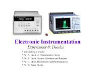
Experiment 8: Diodes * Introduction to Diodes * Part A: Diode i-v Characteristic Curves * Part B: Diode Circuits: Rectifiers and Limiters * Part C: LEDs, Photodiodes ...
| PowerPoint PPT presentation | free to view

ripple voltage, Vr and. Vr Q/C (L22) Eliminating Q from (L21) ... Capacitor size is half that of the half-wave case for the same load current and ripple voltage ...
| PowerPoint PPT presentation | free to view

3 Diode * EEE270 Electronic engineering EEE270 Electronic engineering EEE270 Electronic engineering EEE270 Electronic engineering EEE270 Electronic ...
| PowerPoint PPT presentation | free to view

k = Boltzman's constant = 1.38 x 10⁻²³ joules/kelvin. T = absolute temperature ... ? = constant dependent on structure, between 1 and 2 (if not given assume n = 1) ...
| PowerPoint PPT presentation | free to view

Explain and analyze the operation and characteristics of power supply ... of diode limiters. Determine the output voltage of a biased limiter ... Limiters ...
| PowerPoint PPT presentation | free to view
This voltage is like the voltage required to power some electrical device. ... The i-v characteristic can be checked by building the circuit and measuring the ...
| PowerPoint PPT presentation | free to download

PN Junction / DIODE * Bollen * * * * * * * * * * * AGENDA Bollen SEMICONDUCTOR Pure silicium P material boron doped N material stibium doped P material and N material ...
| PowerPoint PPT presentation | free to view
Ideal Diode Model Real PN Junction Diode I-V Characteristic Mobile Carriers What happens when P-type meets N-type? E-field and Built-in Potential Junction Built-In ...
| PowerPoint PPT presentation | free to download

A Full Wave Rectifier Full Wave Rectifier With Smoothing Rectifiers and DC voltage If a time-varying voltage is only positive or only negative all of the time, ...
| PowerPoint PPT presentation | free to download

TG3: Diode Read-out and signal processing C. Cattadori on behalf of the working group Choice of FET and preamps Choise of FET and preamps Analog electronics Choice of ...
| PowerPoint PPT presentation | free to download

By means of the transferred electron mechanism, it has the negative resistance characteristic ... high frequency operation and Medium RF Power characteristic ...
| PowerPoint PPT presentation | free to view

This barrier simulates the behavior of a pn-junction. Recovery charge of this diode is much less than the equivalent pn-junction diode. ...
| PowerPoint PPT presentation | free to view

Analog Electronics. Faculty of Electrical & Electronic Engineering, KUKTEM ... FIGURE 3-53 Basic schematics of the IR emitter and IR detector circuits. ...
| PowerPoint PPT presentation | free to view

Diode As Circuit Elements Section 3.1-3.3 Key Concepts Diode models Exponential model Derivation of n Ideal model Constant-voltage model Choosing a Diode Model Use ...
| PowerPoint PPT presentation | free to view

This article discusses what is a photodiode, working principle of photodiode, modes of operation, features, V-I characteristics and its applications
| PowerPoint PPT presentation | free to download

DAC, Diodes, Triacs ME 6405 Intro to Mechatronics Student Lecture Kevin Johnson Minh Vo Lam Duong Wye-Chi Chok Important in selecting a DAC * Max voltage if not ...
| PowerPoint PPT presentation | free to view

Diode in Digital Logic Design Section 3.1-3.3 Schedule # Date Day Topic Section 1 1/14 Tuesday Diagnostic Test L 1/14 Tuesday Lab protocol, cleaning procedure, Linus ...
| PowerPoint PPT presentation | free to download

The Business Research Company offers laser diode research report 2023 with industry size, share, segments and market growth
| PowerPoint PPT presentation | free to download
Anneal sample as before (1600 for 30 min) Remove Carbon Cap (RIE with O2) ... Channel mobility: 40- 45 cm2/Vs (on epilayer layer annealed at 1600 C) Stable up to 15V ...
| PowerPoint PPT presentation | free to download

Electronics Tutorial (Thanks to Alex Pounds) Electronics Tutorial ... IR = (VS VZ) / R. 12/4/09. Electronics and Telecommunications. 9. Zener (continued) ...
| PowerPoint PPT presentation | free to view
... the voltage required to power some electrical device. It is used up turning the device on so the voltages at the two ... What is an i-v characteristic curve? ...
| PowerPoint PPT presentation | free to download

Laser Diode Photoacoustic Detection
| PowerPoint PPT presentation | free to view

The Business Research Company offers visible and uv laser diode market research report 2023 with industry size, share, segments and market growth
| PowerPoint PPT presentation | free to download

Figure 8.43 Full-wave rectifier current and voltage waveforms. 10. 5. 0. 0.005. 0.01. 0.015 ... Figure 8.44 Full-wave bridge rectifier. IC. Rectifier. a. b. c ...
| PowerPoint PPT presentation | free to view

Crystals formed on a photographic plate (few % -- thus the end of chemical ph'y) ... Photo at right is oscilloscope trace showing ~2ns rise time to a single electron ...
| PowerPoint PPT presentation | free to view

Wavelength is long compared to geometry of the substrate and much of the ... 3. Maximum power dissipation ( ) 4. Maximum permissible peak current ...
| PowerPoint PPT presentation | free to view

PN Junction Diodes
| PowerPoint PPT presentation | free to view

Describe how the properties of a semiconductor differ from ... Doping and Impurities (Donors or Acceptors) P-type and N-type Material. 7. 6-2 Junction Diode ...
| PowerPoint PPT presentation | free to view

Logic Families and Their Characteristics 1 Objectives You should be able to: Analyze internal circuitry of a TTL NAND gate for both HIGH and LOW output states.
| PowerPoint PPT presentation | free to view

3. Analyze and design simple voltage ... DC Restore or Clamping Circuit ... Photo Exposure Tool. Early 1990's version. Modern tools are much more complex ...
| PowerPoint PPT presentation | free to view

Bode example. Introduction. Slew-Rate. Figure 3.3 (a) Rectifier circuit. (b) Input waveform. ... Bode example. Introduction. Slew-Rate. Look page 148-150 for ...
| PowerPoint PPT presentation | free to view

EEL Chip size: 500 x 500 x 100 um3. 8/22/09. Chang-Hasnain. 5. p-DBR. n-DBR. gain medium ... Fabry-Perot EEL vs. VCSEL. Gain. Free Spectral Range. 500 mm ~2mm ...
| PowerPoint PPT presentation | free to view