Bandstructures PowerPoint PPT Presentations
All Time
Recommended
Electronic Bandstructures Information from Kittel s book (Ch. 7) + many outside sources. Some lectures on energy bands will be based on those prepared for
| PowerPoint PPT presentation | free to download
Density Functional Theory: a first look. Patrick Briddon ... This is an astonishing statement! Why? i.e. one-to-one relationship. 1st Hohenberg Kohn Theorem ...
| PowerPoint PPT presentation | free to download
International Max-Planck Research School. Theoretical Methods for Surface Science ... Interpolate DG(T,p0) from tables. Reuter and Scheffler, PRB 65, 035406 (2002) ...
| PowerPoint PPT presentation | free to view
Electrons in crystal obey the Newton's law when the external force and its ... ball' Newtonian mechanics because m* accounts for the effect of crystal forces ...
| PowerPoint PPT presentation | free to view
K M G Surface BZ Schockley surface state Tamm state Ediss Eads Physisorption well Chemisorption well Activation barrier Energy z ma a Host Definition of ...
| PowerPoint PPT presentation | free to download
You are in an area of study that has the potential to produce vast ... Rhodes, Verity, Braid, Hector, HPCx, ... Other machines are designed to store files: ...
| PowerPoint PPT presentation | free to download
The influence of other atoms to the total crystal potential is treated as a ... Generally, only contributions from the nearest neighbor atoms are considered. ...
| PowerPoint PPT presentation | free to view
Electronic Properties of PbTe/CdTe (100) interfaces. Roman Leitsmann, F. ... zinc blende structure. fundamental gap at G-point: 1.6 eV. PbTe : CdTe : CBO 1.0 eV ...
| PowerPoint PPT presentation | free to view
plane av.potential. position along [100] PbTe(rocksalt) CdTe(zincblende) 10/3/09 ... green- [110] direction. red - [001] direction. experimental data. 10/3/09 ...
| PowerPoint PPT presentation | free to view
Hansang Bae, Steve Clark, Gerhard Klimeck, Sunhee Lee, Maxim Naumov, Faisal Saied,
| PowerPoint PPT presentation | free to view
Describe crystal by small unit cell, which. is repeated in all 3 dimensions ... Industries (Canon, Eastman, Exxon, Fuji, A.D.Little, Mitsubishi, Motorola, NEC, ...
| PowerPoint PPT presentation | free to download
Bond-Order Potential for MD Simulation: Relaxation of Semiconductor Nanostructures tight binding and bond order 4th moment approximation parameterization and fit
| PowerPoint PPT presentation | free to view
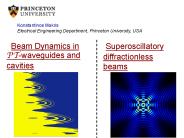
Konstantinos Makris Electrical Engineering Department, Princeton University, USA Superoscillatory diffractionless beams Beam Dynamics in PT-waveguides and
| PowerPoint PPT presentation | free to download
Tight-binding molecular dynamics study of mechanical and electronic properties in twisted graphene nanoribbons Satofumi Souma, Shozo Kaino, and Matsuto Ogawa
| PowerPoint PPT presentation | free to view
Optics on Graphene Graphene (A Monolayer of Graphite) Optical Studies of Graphene Graphene Band Structure of Monolayer Graphere Exfoliated Graphene Monolayers and ...
| PowerPoint PPT presentation | free to download
Spin transport in spin-orbit coupled bands Intrinsic contributions Qian Niu University of Texas at Austin
| PowerPoint PPT presentation | free to view
WIEN2k software package An Augmented Plane Wave Plus Local Orbital Program for Calculating Crystal Properties Peter Blaha Karlheinz Schwarz Georg Madsen
| PowerPoint PPT presentation | free to download
S. V. Khare Department of Physics and Astronomy University of Toledo, Ohio 2. Department of Electrical Engineering and Computer Science University of Toledo, Ohio
| PowerPoint PPT presentation | free to download
... (PDOS) DOS for Graphene PDOS for Graphene Surfaces Surface energy Modeling Surfaces Modeling Surfaces Modeling Surfaces Convergence of slab models Quantum size ...
| PowerPoint PPT presentation | free to download
Activity 1 : Introduction to CCDs'
| PowerPoint PPT presentation | free to download
... if there is extra symmetry: 2. Inversion (P) Symmetry : determined by Parity of occupied ... inversion symmetry of pure Bi, Sb (Fu,Kane PRL'07) Experiment: ...
| PowerPoint PPT presentation | free to download
NASA radiation and temperature requirements are. outside commercial and military interest ... NASA Relevance: 2-5mm Lasers and detectors ...
| PowerPoint PPT presentation | free to view
Title: PowerPoint Presentation Author: Nichols A. Romero Last modified by: Amy Young Created Date: 6/15/2002 2:29:35 AM Document presentation format
| PowerPoint PPT presentation | free to download
Hagen, Ch. Hendlmeier (Regensburg) L. Forr , E. Ljubovic (Lausanne) ... Introduction: Electronic structure of carbon nanotubes. Quantum interference ...
| PowerPoint PPT presentation | free to download
and Topological Band Theory. The Quantum Spin Hall Effect. and ... II. Two Dimensions : Quantum Spin Hall Insulator - Time reversal ... Antiparticle : ...
| PowerPoint PPT presentation | free to view
Physically-Based Analytic Model for Strain-Induced Mobility Enhancement of Holes ... Typical Case: Sxx and Szz stress in [110] and perpendicular direction ...
| PowerPoint PPT presentation | free to download
Quasi Symmetric Moderate Refractive Index Photonic Crystal Waveguides on Mesoporous Substrates Markus Schmidt, Gunnar B ttger, Christian Liguda, Dion Klunder and ...
| PowerPoint PPT presentation | free to download
OE_50200: Compound Semiconductors. Jim Y. Chi(???) ????????. National Dong-hua University, ... What is the Moor's law for Compound Semiconductor technology? ...
| PowerPoint PPT presentation | free to view
Tight binding approach to incorporate accurate bandstructure in nanoscale device ... Advantages of empirical tight-binding models: ...
| PowerPoint PPT presentation | free to view
Luminescence spectrum depends on Si concentration. red-shift for larger nanocrystal size ... from D. Vanmaekelbergh. Luminescence from compound semiconductor ...
| PowerPoint PPT presentation | free to view
FFLC Seminar: Place Position in the Publication Process Equipping yourself with the tools to succeed in the world of the peer-reviewed scientific journal
| PowerPoint PPT presentation | free to download
III. Applications: iii) Ternary alloys. Stoichiometric composition X2YZ ... iii) Ternary systems. iv) Layered structures. Clean V(001), Cr(001) and Fe (100) surfaces ...
| PowerPoint PPT presentation | free to view
Next Generation Electronics from Silicon Carbide to Carbon Nanotubes and Smart Sensors: Paradigms for UMD-ARO/ARL Collaboration Neil Goldsman Dept. of Electrical and ...
| PowerPoint PPT presentation | free to download
(rc, kc) (rc, kc) (rs, ks) Macroscopic densities. Spin density. Torque density ... Generally nonzero in inversion asymmetric crystals. L. S. Levitov et al., Sov. Phys. ...
| PowerPoint PPT presentation | free to view
For free electron in metals: U 0 because of high electron density ... Mean Free Time: Mobility: 27. Carrier-Phonon Scattering. Phonon modulates the periodic potential ...
| PowerPoint PPT presentation | free to download
Non-equilibrium Green's function formalism (Keldysh-LB) Advantages: ... Well established formalism valid in linear and nonlinear regime ...
| PowerPoint PPT presentation | free to view
valence electrons. E. x. International Max-Planck Research School ... potential method, since only the valence electrons are treated explicitly, but ...
| PowerPoint PPT presentation | free to view
K. Nehari et al., Solid-State Electronics, 50, 716 (2006) ... of the Ion current delivered by a LG=9nm nanowire MOSFET as a function of ...
| PowerPoint PPT presentation | free to view
Quantum Transport at the Nanoscale Kristian Sommer Thygesen Center for Atomic-scale Materials Design (CAMD) Technical University of Denmark Calculating parameters for ...
| PowerPoint PPT presentation | free to view
Scaling Issues in nanometer MOSFETS. Parasitics the ultimate showstoppers. Project relevance ... Tools of the trade what we need. Bandstructure. Self ...
| PowerPoint PPT presentation | free to download
Nanoscale Analytics
| PowerPoint PPT presentation | free to view
Towards Utilizing Spontaneous Coherence in Bilayer Graphene for Ultra ... of two monolayers of graphene separated by a tunnel oxide with local gates to control ...
| PowerPoint PPT presentation | free to download
University of Illinois, April 31 - May 1 ... Phase matching wase used using the modal dispersion of the waveguide. QC Laser Highlights ...
| PowerPoint PPT presentation | free to view
Carrier velocity and maximum attainable current IBL ... (far from equilibr. transport) Provide sound interpretation to characterization ...
| PowerPoint PPT presentation | free to view
Tutorial on Electronic Transport
| PowerPoint PPT presentation | free to view
Czochralski process for creating monocrystalline silicon ingots ... Kerf loss. Disadvantages: Lower electronic quality. Increased fragility ...
| PowerPoint PPT presentation | free to view
Ab initio Calculation of Structural and Electronic Properties of Interfaces ... preconditioned residuum-minimization method for the. electronic relaxation ...
| PowerPoint PPT presentation | free to view
for wavelength of 8-10 m. Conclusion. 4. Laser types and covered ... Shorter wavelength, l~7.8 mm (larger confinement GAR, smaller losses aw) Improved design: ...
| PowerPoint PPT presentation | free to view
Absorption spectrum of oriented transpolyacetylene ... Frist Brioullin zone. Contains all necessary. information, -p/L -3p/L -5p/L. Second Brioullin zone ...
| PowerPoint PPT presentation | free to view
Professor Martti Puska and Karri Saloriutta. Professor Antti-Pekka Jauho. Dr (Tech) Ari Harju ... Chen et. al. arXiv:cond-mat/0701599 ...
| PowerPoint PPT presentation | free to download
How is the Band Gap formed? For free electron in metals: U 0 because of high electron density ... Occupation of donors by electrons: Occupation of acceptors by holes: ...
| PowerPoint PPT presentation | free to download
Monte Carlo studies of the transient response of electrons and phonons in cubic InN ... http://www.emrs-strasbourg.com/files/pdf/2004_SPRING/book_of_abstract/ABSL. pdf ...
| PowerPoint PPT presentation | free to view
Re-spin designs to respond to system's needs; fabricate & deliver new modules. Unique features ... Fabricate & test device arrays ...
| PowerPoint PPT presentation | free to view
TBPW: A Modular Framework for Pedagogical Electronic Structure Codes ... Implemented using a rotation matrix formalism allows the use of orbitals with ...
| PowerPoint PPT presentation | free to download
Gallium Nitride and III-Nitride Semiconductors. III-Nitride Semiconductors. Evolution of Luminous Efficiency by Technology. GaN ... GaN/Sapphire Growth ...
| PowerPoint PPT presentation | free to view


