Word Line Driver - PowerPoint PPT Presentation
1 / 16
Title:
Word Line Driver
Description:
Word Line Driver Last stage of row decoding typically decodes only 1-address line (1/2 decoder) because the final stage must be sized to drive the word line load ... – PowerPoint PPT presentation
Number of Views:112
Avg rating:3.0/5.0
Title: Word Line Driver
1
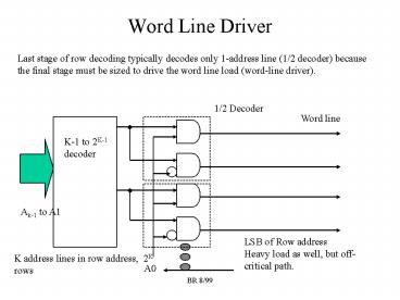
Word Line Driver
Last stage of row decoding typically decodes only
1-address line (1/2 decoder) because the final
stage must be sized to drive the word line load
(word-line driver).
1/2 Decoder
Word line
K-1 to 2K-1 decoder
Ak-1 to A1
LSB of Row addressHeavy load as well, but
off-critical path.
K address lines in row address, 2K rows
A0
2
Mitsubishi 4 Mbit SRAM
- 4Mb x 1, 222 bits, 22 address lines
- A single square array would be 211 rows x 211
columns, each word line would have 2048 RAM cell
loads!! - Use hierarchical decoding to break large array
into smaller arrays - Use 32 blocks
- Each block is 1024 rows x 128 columns 128Kb
- 128Kb x 32 217 x 25 222 4 Mb.
- 7 bits for column decode (128 columns). Remaining
bits (15) for block (5), row decode (10).
3
Decoding Scheme
A21..A12 A11 A10A9A8
A7 A6...A0
Row(10) Left/Right (1) Pre-blk-dec(3)
Fblk(1) Col(7)
A11
3 to 8
A10..A8
En 10 to 1024
En 10 to 1024
En 1 to 2
En 1 to 2
En 1 to 2
1024 rows x 128 col block
A7
A21..A12
16 blocks on each side
4
Decoding Scheme, another View
A11
Row
0
511
En 10 to 1024
1023
1 to 2
1 to 2
A7
A7
1
A21..A12
0
3 to 8
A10 A9 A8
5
Loading
- On 10 to 1024 decoder outputs
- 8 loads (16 blocks divided into 8 groups of 2)
- On 3 to 8 decoder outputs
- 1024 loads
- On 2 to 1 decoder outputs
- 1024 loads
Want to equalize delay paths complex decode
light load small decode large load 10 to
1024 8 loads 3 to 8
1024
6
Critical Decode Path
A11
off path 7 loads
Word line 128 Ram cell loads
off path 1023 loads
En 10 to 1024
1 to 2
A21..A12
A7
Should match 3to8 delay to 10to1024 delay.
off path 1023 loads
3 to 8
A10 A9 A8
7
Cypress 1 Mb Dual Port RAM
- Arranged 64K x 16
- Array split into 32 blocks, each 512 rows by 64
bits (4 words of 16) - 16 sense amps per block, 1 sense amp per bit
shared among 4 words - 32 blocks x 512 rows x 64 bits 25 x 29 x 26
220.
Plane(1) Max WL(9) Min WL(2) Row Grp(2)
Col(2)
A15 A14..A6 A5A4 A3 A2
A1..A0
8
A15
Plane 1
16 blocks/plane
Plane 0
2 to 4
A5A4
MinWL
2 to 4
RowGrp
A3A2
A14
Row (64 bits)
8 to 256
A13...A6
9 to 512
9
Loading
- on 8 to 256 decoder output (2 loads)
- on A14 (512 loads)
- on 9 to 512 decoder outputs (16 loads)
- on 4 to 16 decoder (combined Min WL Row Grp)
- 512 loads
- On final wordline driver output (64 SRAM loads)
Delays Want Dx 8 to 256 decoder A14 (512
loads)Want Dy 4 to 16 decode (512 loads) 9
to 512 (64 SRAM bit loads)
10
Misc Comments
- The plane bit is not involved in the Major Word
line decoding. - Both Major Row decoders active but still only one
final word line is active - Physical layout had Row Group and Min WL lines
running down the center of the chip with planes
on left/right side
11
0
1
2
3
62
63
60
61
512 Rows x 64 Columns
A1 A0
4/1 Pass Transistor Decoding
16 Sense Amps
16 bit block output
Block Column Decode
12
BLK0
BLK1
BLK2
BLK30
BLK31
16
16
16
16
16
2 to 1
0
1
14
15
Plane Select (A15)
16
16
16
16
16 to 1
Min WL A5 A4
Row Group A3 A2
16
Data out
Word Selection
13
Fast Decoders
Need Fast, Wide Decoders for Row Decode. Because
of large number of inputs, use a NOR form with a
static pullup or precharged pullup.
An/An
An-1/An-1
A2/A2
A1/A1
14
Fast Decoders (cont)
Precharge
An/An
An-1/An-1
A2/A2
A1/A1
Precharge can be generated from clock or address
transition detection logic.
15
Power Decoded NOR
A
B
Out
A
B
C
A NOR gate version that saves power.
16
Address Transition Detection (ATD) Logic
A0
delay implemented as chains of inverters
NOR with static pullup inverter
A1
AN-1
Any change on address lines generates an output
pulse, can be used for precharging.


