
Intensity%20(counts/s) - PowerPoint PPT Presentation
Title:
Intensity%20(counts/s)
Description:
Intensity countss – PowerPoint PPT presentation
Number of Views:121
Avg rating:3.0/5.0
Title: Intensity%20(counts/s)
1
Nanostructures and Materials
Intensity (counts/s)
y (micron)
Condensed Matter
2
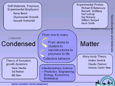
CONDENSED MATTER EXPERIMENT
- Rama Bansil
- Michael El-Batanouny
- Bennett Goldberg
- Karl Ludwig
- Raj Mohanty
- William Skocpol
- Kevin Smith
- Other Physics faculty with primary appointments
in other departments
3
He-Scattering Facility Michael El-BatanounyDOE
4
Magnetic Domain Formation
5
- NSF
- DOE
- ARO
6
(No Transcript)
7
(No Transcript)
8
(No Transcript)
9
(No Transcript)
10
(No Transcript)
11
(No Transcript)
12
(No Transcript)
13
(No Transcript)
14
Karl Ludwig X-ray Group Real-Time X-ray
Studies of Materials Processes
Lock-in 1
1013 ?/sec E? 6.9 keV
Laser
Lock-in 2
Laser
Multilayer
Focusing
Position
Monochromator
Synchrotron
Mirror
Sensitive
X20C
Detector
NSLS
Linear
- 14 range in 2?
- 30ms time resolution
X-ray Detector
Sample
Annealing
Chamber
Beamline
Measurement
Control
and Control
Electronics
Experiment
Analysis
Control
Workstation
LabVIEW
15
- Growth of C54 TiSi2 Phase Used in Semiconductor
Industry - (collaboration with IBM Research)
27 nm Ti
16
- Development of Surface Nanostructures During Ion
Bombardment (collaboration with Naval Research
Lab)
Evolution of x-ray scattering during ion
bombardment showing formation of surface
nano-structures
AFM image after ion bombardment showing formation
of nanodots
- Growth of III-V Nitride Semiconductors by
Molecular Beam Epitaxy (collaboration with
Moustakas Electrical Engineering)
17
An In-situ UHV Materials Processing Facility at
National Synchrotron Light Source NSF, DOE
- Real-time X-ray Studies of
- III-nitride thin film growth by MBE
- Surface evolution during sputter erosion and
plasma exposure - Ultra-thin (lt 10 nm) silicide film formation
Co-Si, Ni-Si
18
Biological and Synthetic Nanoscale Structures
formed by Macromolecules
Rama Bansil NSF
- Microscopy
- Light Scattering
- Small-angle X-ray Scattering
- Small-angle Neutron Scattering
19
Bennett Goldberg Nano-optics of Quantum
Structures
- Simultaneous electronic and optical quantum
confinement - Manipulate the electronic excitations with
optical fields, D lifetime, spin, coupling - Quantum computing, nanoscale electronics,
photonics
20
Low-Temperature Near-field Scanning Optical
Microscopy
- Self Assembled Quantum Dots
- Small (10-20nm) - Confinement Coulomb energy
- Virtually defect free - very high quantum
efficiency - Homogenous size distribution
- Self - assembly, Straski-Krastanov growth
Atomic-like emission due to 3D quantum confinement
Ensemble of 30 self-assembled quantum dots
measured by 100nm near-field tip at 4K
Emission Intensity (a.u.)
homogeneous linewidth lt 0.1 meV
1850
1900
1950
2000
Energy (meV)
21
- Spatial spectroscopy scans
- Build 3D data set x - y - l, -- then take
slices at specific l
l -- scan through emission line of dot in center
- Imaging a single quantum dot
Intensity (counts/s)
doughnut shape due to tip shadowing
1.0
y (micron)
1889.68 meV
0.8
0.6
y (micron)
0.4
0.2
size of tip
0.0
0.0
0.2
0.4
0.6
1.0
0.8
x (micron)
streaks due to spectra diffusion
22
Spectral diffusion in an individual quantum dot
during spatial scan
- Each image 500nm square
- Scan takes 4 hours, thus read pixels across as
time sequence
Absence of emission at these spatial points (read
time) appears at a lower emission energy above
- During scan, placing single electron within 5nm
of dot creates spectral stark shift of exciton - Summing spectral energies integrates over time
and removes streaks
peak
23
- Quantum Information
- Quantum-Classical Transition
- Fundamental properties of
- Metals, Insulators, Superconductors
Electronic Systems
PHYSICS WITH NANOSTRUCTURES
Mechanical Systems
- Quantum Mechanical Oscillator
- Dissipation and Quantum Friction
- Fundamental Force Measurements
- with Micromechanical Structures
- Quantum regime of heat flow
Laboratory for Nanoscale Research, Prof. Raj
Mohanty
Prof. William Skocpol
24
Nanoscale Electronic
Nanoscale Mechanical
Structures Structures Advanced
E-beam lithography surface micromachining
Quantum Dissipation Energy relaxation
in Micro-electro-mechanical Systems
(MEMS) Force Detection Nanoscale Antenna
Mechanical sensor for ultrasmall force
detection (DNA, Gravity,tunneling) a single
electron Quantum Friction Mechanical (friction)
force, due to the tunneling of a handful of atoms
Quantum Decoherence Coherent electrons over 25
mm and 80 ns Schrodingers Kitten (8 mm
loop) Persistent current from a single
electron Berry Phase Spin rotation of
single Electron (by p/6) about another localized
spin
25
Problems being addressed in the Lab
Electronic Structures
Mechanical Structures
- How to fabricate, control
- manipulate a quantum bit
- to create coherence and
- (EPR) entanglement
- How to control reverse
- quantum decoherence in
- any quantum system
- How do the nanoscale
- high-Tc superconductors
- behave
- What determines energy loss
- (quantum dissipation) in
- Nano- or Micro-Electro
- Mechanical Systems
- Is the Newtons inverse-square
- law of gravity valid in micron
- distance scales
- (Do extra dimensions exist)
- Does heat flow in nanoscale
- structures occur according to
- quantum mechanics
Laboratory for Nanoscale Research, Prof. Raj
Mohanty
26
Physics Research in Affiliated Areas
Quantum Optics, Biomedical Optics,
Ultramicroscopy, Device and Materials Physics,
Nanoscience, Nanobiotech Ted Moustakas ECE Selim
Ünlü ECE Alexander Sergienko ECE Bahaa Saleh
ECE Mal Teich ECE Irving Bigio BME Evan Evans
BME Kamil Ekinci AME Todd Murray, AME Tejal
Desai, BME
27
QUANTUM IMAGING LABORATORY at Boston University
CO-DIRECTORS B. E. A. Saleh, A. V. Sergienko,
M. C. Teich http//www.bu.edu/qil
28
Parametric Down Conversion - source of entangled
states
-Photons 1 and 2 have the same polarization and
traverse the same direction
-Photons 1 and 2 have orthogonal
polarizations and travel different directions
29
Quantum Ellipsometry
- Makes use of polarization-entangled photon pairs
generated from type-II - spontaneous parametric down conversion.
- -Interferometric scheme in conjunction with using
two-photon source - provides a natural self-referencing.
- -A reference sample need not be used for
ellipsometric measurements.
30
Proposed Applications
Quantum Information and Communication, Quantum
Networking multiparty secure quantum key
distribution (quantum cryptography). (In
cooperation with Tom Toffoli and Lev Levitin at
BU).
Quantum Imaging (Spatial Entanglement at Work)
designing imaging configurations for
unconventional practical applications.
Quantum Ellipsometry characterization of surface
properties of semiconductors, and materials used
in optoelectronics.
Quantum Optical Tomography (of real objects) do
not confuse with tomography of quantum states.
The feasibility of cryptography, metrology, and
imaging has been demonstrated experimentally in
our laboratory and experiments demonstrating
ellipsometry, microscopy, tomography, and
holography are underway.
31
Near field and Picosecond Spectroscopy
M. Selim Ünlü, B. B. Goldberg Anna Swan
- Ultramicroscopy
- Material Characterization
- GaN - time-resolved spectroscopy
- Scanning probe microscopy
- NSOM
- Waveguides, biosensing
- Thermal Imaging
- Photodetectors
- HYPX MRI
DARPA, NSF, ONR, ARO, NIH
32
NANO OPTICS
- High spatial resolution subsurface microscopy
- Quantum Dot Spectroscopy
Goldberg Ünlü
33
NAIL Numerical Aperture Increasing Lens
34
Comparison of Confocal to Tip-Enhanced in Raman
Microscopy of Carbon nanotubes
35
Raman scattering in a nutshell
Lattice vibrations
Stokes
Anti-Stokes
?scattered
?laser
Energy units for optical spectroscopy 1/? (cm-1)
Energy and momentum conservation
1/? wavenumber 500 nm 20 000 cm-1 300 cm-1
37.2 meV
36
Resonant Raman Scattering
- Laser light in to illuminate at most one tube at
a time - Only tubes in resonance with light will interact
start to vibrate (or give up vibration energy
to light) - Signallaser ? vibration energy from resonant
tubes
Measures the properties of an individual tube
G
37
SWNT on a Substrate with Grid
AFM image
wRBM185cm-1 dt1.34nm
Lithography Steve Cronin, Harvard
38
SURFACE ENHANCED VIBRATIONAL SPECTROSCOPY AND
MICROSCOPY
Carbon nanotubes
- well defined topography - large sRaman -
resonance enhancement
Phys.Rev.Lett. 90, 95503 (2003)
39
NEAR-FIELD RAMAN IMAGING OF CARBON NANOTUBES
topography
Raman scattering
line-scan
40
Self Interference of fluorescent light
- Self interference between directly emitted and
reflected light interferes constructively or
destructively depending on wavelength and height
over mirror.
41
Fluorescein on surface and on top of
StreptavidinDemonstration of better than 5 nm
vertical resolution
42
Wide Bandgap SemiconductorsLaboratory
- Theodore D. Moustakas
- In this laboratory we address materials and
device physics issues of the wide bandgap
semiconductors InN, GaN, AlN and their alloys and
heterostructures. Current projects are related to
making visible and ultraviolet LED and laser
structures, solar-blind, UV photodetectors,
electronic devices (diodes, transistors,
thyristors) and MEMS sensors. - The materials and devices are grown by molecular
beam epitaxy (MBE), vapor phase epitaxy (VPE) and
gas cluster ion-beam deposition (GCIB).
Wide Bandgap Semiconductors Lab
BOSTON UNIVERSITY
43
(No Transcript)
44
(No Transcript)
45
(No Transcript)
46
Laboratory for Nanometer Scale Mechanical
Engineering
- Kamil L. Ekinci
- ekinci_at_bu.edu
47
Nanomechanics at BU
- Focus areas
- Surface analysis and engineering of
nanostructures at the atomic scale - Nanoelectromechanical Systems (NEMS) sensors and
signal processing components
High frequency NEMS
Experimental set up UHV Surface analysis chamber
Silicon atoms on the surface of a device
48
NEMS to measure single molecules
Nanomechanical system moves nanometers at ultra
high frequency gt Sensitive to tiny amounts of
material
magnetomotive actuation and transduction
- single molecule detectors
- single molecule chemical sensors
- mass spectrometry
Kamil Ekinci
49
What are nanomachines good for?
- Unprecedented sensitivities
- Ultrafast electromechanical devices
- Sensors sensitive to single molecules
- Capable of detecting tiny forces
- Interesting Physics
- Mesoscopic and molecular limit to mechanics
- No longer at the classical limit,
- quantum mechanics take over.
- No longer at the thermodynamic limit, atomistic
processes are important
50
AME Laser Acoustics Lab Photoacoustic and
Photothermal (PA/PT) Characterization at the
Nanoscale
PA/PT techniques well suited for
materials characterization at the macro/micro
scales but spatial resolution limited by
diffraction
Laser interaction with materials physical
processes used in photoacoustic and photothermal
microscopy.
Evaluation of thermomechanical properties of
nanoscale systems through photoacoustic and
photothermal microscopy requires higher
resolution Nearfield Optical Techniques
High resolution photoacoustic and photothermal
microscope in the Laser Acoustics Lab.
Research part of NIRT effort
51
Photothermal and Photoacoustic Characterization
of Nanoscale Systems
Plasmon resonance in nanoparticles may help us to
localize the excitation laser energy
Nanomechanical resonators fabricated at BU
(Ekinci)
We are currently evaluating the use of PA/PT to
measure the thermal and mechanical response of
nanoelectromechanical systems (NEMS)
Supported through NSF NER
52
BOSTON UNIVERSITY
Nanotechnology Research _at_ Bennett
Goldberg Electrical and Computer
Engineering Physics
selim_at_bu.edu goldberg_at_bu.edu
53
Material Synthesis Device Fabrication
- Optoelectronics Processing Facility
- Lightwave Technology Laboratory
Ekinci, Moustakas, Mohanty
54
5 ?m Nanoporous Silicon (pSi) Particles
Applications in Biology and Biomedical
Engineering Nano-Bio-Technology
- High Resolution Biological ImagingInterdisciplina
ry Research Teams
Volume (Particle) 68 fL Volume (RBC) 76 100
fL
Desai Tien
55
Why Therapeutic Nanotechnology?
- Significant unmet medical needs
- Nanoscale features mimic biological world
- Unprecedented control over features (surface
chemistry, topography) - Targeting and localization
- Self-regulation (sensing transduction)
- Novel Materials
- MULTI-FUNCTIONALITY
56
Fiction Nano-robots or the Fantastic Voyage
57
Fact Non-Invasive Deliveryof Peptides and
Proteins
- Lectin coating
- adheres to intestinal mucosa
- Nano-reservoirs
- Filled with EPO ( ) and enhancer ( )
lyophilized - Drug released close to intestinal cells
- Locally high concentrations to enhance
paracellular transport
1.5 microns
.5 microns
58
Future Integrated Drug Delivery Nanosystems
Biosensors
Sensor Interface
Tumor Targeting
Molecule, Cell
Encapsulation
Reservoir
Packaging
Power
Supply
Nanopores
Antenna
Actuator
Control Electronics
Interconnect
Fantastic voyage?
59
Potential Target Diseases/Therapies
Disease Drugs Sales
Chronic hepatitis C Alpha interferon 1.5 billion
Anemia EPO 4.7 billion
MS Beta Interferon 1.6 billion
Neutropenia G-CSF 1.9 billion
Psychosis Anti-psychotics 4.0 billion
Diabetes insulin 4.0 billion
Cancer chemotherapy 20 billion
60
Center for Nanotechnology Integration
61
NANOTECHNOLOGY
Life Sciences
Physical Sciences
Tissue EngineeringTejal DesaiEvan EvansRussell
GiordanoCatherine KlapperichJoe TienJoyce Wong
Electronics/Optics/ITNeed Identified Enrico
BellotiThomas BifanoKamil EkinciShymasunder
ErramilliBennett GoldbergRaj MohantyTed
Morse Ted Moustakas Bahaa SalehAnna SwanSelim
Ünlü
Biomimetic MaterialsTejal DesaiRussell
GiordanoCatherine KlapperichJoe TienJoyce
WongXin Zhang
CharacterizationRama BansilBennett
GoldbergTodd MurrayAnna SwanSelim Ünlü
Smart DevicesThomas BifanoIrving BigioTejal
DesaiKamil EkinciShymasunder ErramilliEvan
EvansMaxim Frank-KamenetskiRosina
GeorgiadisBennett GoldbergRaj MohantyTed
Morse Todd MurrayAnna SwanSelim ÜnlüJoyce
WongXin Zhang
ManufacturingThomas BifanoTejal DesaiKamil
EkinciRaj MohantyAndre SharonJoe TienXin Zhang
Genomics ProteomicsCharles CantorJim
CollinsMichael ChristmanCharles DelisiJim
DeshlerShymasunder ErramilliMaxim
Frank-Kamenetski Rosina GeorgiadisCatherine
KlapperichCassandra SmithZhiping Weng
EnergySrikanth GopalanUday PalVinod Sarin
Materials ScienceKevin Smith Bennett Goldberg
Karl Ludwig M. Selim Ünlü Ted Moustakas
Homeland SecurityBennett GoldbergShymasunder
ErramilliRaj MohantyRanjith PremisiriSelim
Ünlü
BiologyJames Deshler
62
Core Nanoscience efforts at Boston University
- Nano-optics in materials science
- Nanoscale Interdisciplinary Research Team
developing optical techniques for at length
scales of ?/10. NSF - MURI with U of R
- Nano-optics in subcellular bioimaging and
medicine - Using new techniques in interference microscopy
to image fluorophores in vivo with nanometer
resolution. NIHNSF - Nano-electromechanical systems
- Nanosensor arrays for molecular detection using
UHF cantelevers. NEMS for microengines, active
mirrors, rapid and variable genomic and protein
array fabrication - Nano-electronics
- Nanowires, dots, and devices for coherent
transport for secure communications and quantum
computing - Whitaker Laboratory for Micro and Nano Biosystems
- Nanotherapeutics Targeted drug delivery,
nanoporous membranes, smart nanoparticles - Cellular scaffolding, polymer tethers
- 3D self assembly
- Nanomechanics of biosystems Individual chemical
bonds - Dip-pen nanolithography, polymers
- Infrared microscopy to 100nm, femtogram
spectroscopy and breast cancer screening using a
single strand of hair - Biosensing and homeland security
- Surface Plasmon Resonance, Array-based,
multichannel sensors - Ring resonators and fiber-based systems
63
Education in interdisciplinary Nanoscience IGERT
in Micro- and Nano-Biosystems
Core courses in departmental discipline
Augmented by journal clubs, lab rotations, and
bioethics, societal impact, and tech transfer,
seminars
- Core interdisciplinary courses in
Micro/Nanoscience - Physical Phenomena
- Structures and Fabrication
- Measurement and Analysis
Internships at industrial research labs, national
labs, and international centers of excellence.
Existing Advanced courses in Micro/Nanoscience
Chemistry Nanostructured arrays for SPR of DNA
Engineering Nano-photonic devices for DNA sensing
Physics NEMS for single molecule measurements
Dental Nano-composites for tooth replacement
Biology Cells on biomimetic structures
Recommended
CrystalGraphics Presentations


