Design/Verification Process - PowerPoint PPT Presentation
Design/Verification Process
Register, 4-bit, synchronous load and clear. Built from DFFs without load or clear ... Try different relative timings on input signals ... – PowerPoint PPT presentation
Title: Design/Verification Process
1
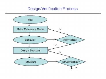
Design/Verification Process
Idea
Make Reference Model
N
Ref Idea?
Behavior
Y
Design Structure
N
StructBehav?
Structure
Y
2
Component Design/Verification Example
Register, 4-bit, synchronous load and clear
- Built from DFFs without load or clear
- What if clear and load are both asserted?
3
Register, Behavioral
always _at_(posedge load or posedge clear or posedge
clock) if (load) Q lt D else if
(clear) Q lt 4b0
- Load has priority over clear
4
Register Testbench, Response Checking
reg_behav r1 (out1, in, clock, load,
clear) reg_struct r1 (out2, in, clock, load,
clear) always _at_(posedge sclock) if (out1 !
out2) display (error)
- Sclock transitions just before clock
- Outputs must settle before clock edge
5
Test Stimulus, Reference Model Response
- 1 bit shown, assume initialized to 0
clk
D
Q
ld
clr
6
New Test Stimulus
- 1 bit shown, assume initialized to 0
clk
D
Q
ld
clr
- Is this waveform correct?
7
Reference Model
always _at_(posedge load or posedge clear or posedge
clock) if (load) Q lt D else if
(clear) Q lt 4b0
- Load and clear are in the sensitivity list
- Reset and clear are asynchronous
8
Testing Rules of Thumb
Bad test stimulus can cause a bug to be
undetected Try different relative timings on
input signals
PowerShow.com is a leading presentation sharing website. It has millions of presentations already uploaded and available with 1,000s more being uploaded by its users every day. Whatever your area of interest, here you’ll be able to find and view presentations you’ll love and possibly download. And, best of all, it is completely free and easy to use.
You might even have a presentation you’d like to share with others. If so, just upload it to PowerShow.com. We’ll convert it to an HTML5 slideshow that includes all the media types you’ve already added: audio, video, music, pictures, animations and transition effects. Then you can share it with your target audience as well as PowerShow.com’s millions of monthly visitors. And, again, it’s all free.
About the Developers
PowerShow.com is brought to you by CrystalGraphics, the award-winning developer and market-leading publisher of rich-media enhancement products for presentations. Our product offerings include millions of PowerPoint templates, diagrams, animated 3D characters and more.


