
Novel Communications Mechanisms - PowerPoint PPT Presentation
1 / 8
Title:
Novel Communications Mechanisms
Description:
optics options (free-space, fibers, waveguides) ... 4. Monolithic and hybrid prototypes to evaluate performance, process compatibility and cost. ... – PowerPoint PPT presentation
Number of Views:87
Avg rating:3.0/5.0
Title: Novel Communications Mechanisms
1
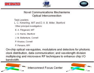
Novel Communications Mechanisms Optical
Interconnection
Task Leaders L. C. Kimerling, MIT and D. A. B.
Miller, Stanford
Other principal investigators E. A. Fitzgerald,
MIT J. S. Harris, Stanford J. M. Ballantyne,
Cornell P. Krusius, Cornell P. Persans, RPI
On-chip optical waveguides, modulators and
detectors for photonic clock distribution, data
communication and wavelength division
multiplexing and microwave RF techniques to
enhance chip I/O bandwidth.
2
ANALYSIS OF OPTICAL INTERCONNECT OPPORTUNITIES
D. A. B. Miller, Ginzton Lab, Stanford
OBJECTIVE To establish which interconnect
functions are best performed optically how best
to perform them
- MILESTONES
- Define target performance metrics for
optoelectronic devices and optics. - Identify implementation path for key functions.
APPROACH Analyze, clock distribution, on-chip
interconnects and off-chip interconnects for
device options (lasers, modulators,
photodetectors) optics options (free-space,
fibers, waveguides) CMOS driver and receiver
circuit issues (power, crosstalk, latency)
100000
100000
t
Compute BW
t
u
Comp BW
10000
u
10000
t
w
Electrical I/O BW
Elec I/O BW
u
t
u
I/O BW
Optical I/O BW
1000
u
t
w
1000
w
u
w
t
Compute Bandwidth (Gbit/s) Gates x
Clock-Speed
I/O Bandwidth (Gbit/s) I/Os x Clock-Speed
100
SIA Predictions
w
u
t
100
w
t
u
10
w
w
10
1
1
0.1
0
0.1
0.2
0.3
0.4
0.5
0.6
0.7
0.8
Line width (microns)
3
SILICON MICROPHOTONICS TECHNOLOGY
L.C. Kimerling, MIT Materials Processing Center
- OBJECTIVE
- To establish an IC compatible process technology
for integration of photonic interconnection with
silicon electronics. - low cost, high yield
- low power dissipation
- high bandwidth
- reduced interconnection density
- MILESTONES
- SiEr LED
- PolySi nanowaveguide
- Integrated CMOS driver/modulator
- Si microresonator devices
- 16x fanout clock signal
- Integrated Optical Data Link
APPROACH To create technology building blocks
under the constraints of conventional fabline, IC
design and systems performance requirements.
SiEr emitter/waveguide structures Si/SiO2
waveguide/modulator/couplers SiGe detectors
4
III-V on SILICON TECHNOLOGYE.A. Fitzgerald,
MIT Materials Processing Center
- OBJECTIVE
- To establish an IC compatible, monolithic process
technology for integration of III-V
optoelectronic devices with Si CMOS - low cost, high yield
- low power dissipation
- high bandwidth
- reduced interconnection density
MILESTONES III-V LEDs and lasers on Si Creation
of a relaxed SiGe/Si co-planar substrate
technology III-V LEDs and lasers on such
co-planar substrates Demonstration of optical
links on Si
APPROACH To create III-V LEDs and lasers on Si
substrates using intermediate SiGe interlayers.
GaAs and InGaAs emitters on Ge/SiGe/Si
substrates development of co-planar SiGe/Si
technology useful for both III-V integration and
SiGe detector integration
co-planar SiGe/Si
GaAs on Si
Ge
5
HYBRID INTEGRATION OF III-V DEVICES ON SILICONJ.
S. Harris and D. A. B. Miller, Stanford Solid
State and Photonics Lab
MILESTONES Demonstration of dense array optical
interconnects with bonding to active CMOS
circuits optimized devices optimized circuit
designs
- OBJECTIVE
- To establish the viability of integration of
optoelectronic devices with finished Si CMOS
circuits through research in - integration processes
- devices compatible with integration
- operating with CMOS voltages and clock speeds
APPROACH Investigate solder bonding
alternative hybrid integration techniques
optimized devices compatible with CMOS circuit
drive (e.g., improved modulators,
detectors) Assess performance of entire link
skew, jitter, latency, power, error rate and
deduce limitations to performance
6
PARALLEL ARRAY TECHNOLOGIES
J. M. Ballantyne and P. Krusius, Electrical
Engineering, Cornell
MILESTONES
OBJECTIVE
To demonstrate the feasibility of on chip multi-
l
l
Monolithic, wavelength selective materials and
MEMS devices.
wavelength sources and detectors for
multiplexed I/O.
Microamp quantum dot VCSEL arrays.
l
Integrated III-V laser/CMOS transmitter.
l
APPROACH
Functional microphotonic devices for routing/
l
reconditioning signals.
l
Wavelength multiplexed, on-chip detectors and
VCSEL lasers.
Efficient,
l
-selective, monolithic receivers
l
GaInP S-K islands with Si lattice constant
Si heteroepitaxy of selective, quantum dot
l
active regions for detectors and lasers.
Demonstrate CMOS process compatibility of
l
monolithic III-V device materials.
Demonstrate III-V emitter/detectors for
l
multiplexed communications.
,
7
NOVEL WAVEGUIDES FOR OPTICAL INTERCONNECTSP. D.
Persans, J. Plawsky, X.-C. ZhangRPI
- OBJECTIVE
- Develop waveguide materials and processing
approaches for on-chip and MCM optical
interconnects. - APPROACH
- Fabricate passive waveguide structures including
horizontal and vertical input and output couplers
and bends, and straight-line waveguides using IC
process compatible polymers and inorganics.
- Focus on large area processing techniques and
materials photosensitive fluorinated polymers,
reactive ion etching, sputtering. - Focus on off-chip light sources with on-chip
modulators. - MILESTONES
- Development of test structures
- Deposition and patterning of photosensitive
polymers.
8
Approaches 1. Analyze approaches and define
likelihood of success. 2. Evaluate optical chip
I/O and clock distribution functions. 3.
Develop CAD tools for device design, component
integration and partitioning of
optics/electronics. 4. Develop materials and
processes for integration on silicon. 5.
Prototype hybrid and monolithic architectural
platforms, and assess the limits of performance
and integration. 6. Develop entry-level
functionality for e-test and MCMs.
Objectives 1. Complete technical analysis of
optical interconnection with design criteria for
speed/power/area tradeoff. 2. Evaluation of
waveguide and free space performance. 3.
Design-stabilized prototypes for early entry
applications such as testing and MCM/PWB
functions. 4. Monolithic and hybrid prototypes
to evaluate performance, process compatibility
and cost. 5. Novel architectures free space
and optical buss prototypes. 6. Demonstration
of GHz clock and data distribution functions.
Recommended
CrystalGraphics Presentations


