Ch. 2: Sequential Circuit Design - PowerPoint PPT Presentation
1 / 22
Title:
Ch. 2: Sequential Circuit Design
Description:
State is permitted to change only at times specified by a clock signal ... 22. Universal Shift Register. Binary Ripple Counter. Timing Diagram (important) ... – PowerPoint PPT presentation
Number of Views:232
Avg rating:3.0/5.0
Title: Ch. 2: Sequential Circuit Design
1
Ch. 2 Sequential Circuit Design
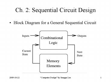
- Block Diagram for a General Sequential Circuit
2
- Types of Sequential Circuits
- Asynchronous sequential
- State is permitted to change at any time
- Synchronous sequential
- State is permitted to change only at times
specified by a clock signal - Memory Devices
- Asynchronous sequential circuits
- Delay element, wire delay, latch, flip-flop
- Synchronous sequential circuits
- Latch level-triggered device (typical usage)
- Flip-Flop edge-triggered device (typical usage)
3
Basic S-R Latch Design
4
Enabled S-R Latch Design
5
D-Latch Design
6
D Flip-Flop, Master-Slave Device
7
J-K Flip-Flop
8
Hazards (due to Races)
Static Hazard
Dynamic Hazard
9
Elimination of Hazards
add consensus term
10
Metastability
- Metastable signals can occur due to unstable data
values during clock signal transitions - Ex
11
Solutions to Metastability
- Metastability can never be completely eliminated
- Try to reduce the likelihood of metastable values
- Possible solutions for asynchronous data inputs
- Use data inputs with extremely fast transitions
- Buffer data through several flip-flops before
using them
12
Synchronous Sequential Circuit Design
- Typically based on Finite State Machines (FSMs)
- Mealy machine
- Outputs depend on the present inputs and the
current state - Moore machine
- Outputs depend on the current state only
- FSM Design Steps(1) Draw a state diagram (or
state table)(2) Make a state assignment(3)
Derive a state transition table(4) Derive logic
equations(5) Derive logic diagram from the logic
equations
13
Counter Example (Prob. 2-16)
- 3-bit synchronous binary counter using D FFs
- Step (1) State Diagram
14
- Step (2) State Assignment
- Use variables (A,B,C) and 3-bit binary assignment
- Step (3) State Transition Table
15
- Step (4) Derivation of Next State Equations
16
- Step (5) Logic Diagram
17
Sequence Detector (Prob. 2-22)
- Design sequence detector (for 1101) using J-K FF
- Step (1) State Diagram
18
- Steps (2) and (3) State Assignment State
Transition Table
19
- Step (4) Derivation of Next State and Output
Equations
20
- Step (5) Logic Diagram
21
Sequential MSI Devices
- n-bit Register
- Shift Register
22
- Universal Shift Register
- Binary Ripple Counter
Timing Diagram (important)


