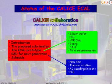
Status of the CALICE ECAL - PowerPoint PPT Presentation
1 / 22
Title: Status of the CALICE ECAL
1
Status of the CALICE ECAL
CALICE collaboration
http//polywww.in2p3.fr/flc/calice.html
- Silicon wafer
- PCB
- VFE Chip
- Gluing
- DAQ
- First measurements
- Introduction
- The proposed calorimeter
- The ECAL prototype
- RD for next generation
- Schedule
- New chip
- Thermal studies
- AC coupling (silicon)
- PCB
2
It is not RD in the back yard !!
3
Start from physics See what design/technique
could fit List the RD to do to validate the
choice Study potential performance with simul.
Optimise EFLOW performances lead to optimize
close showers separability so, like digital
camera ? number of pixel !!!!
4
The proposed calorimeter
Ultra granular/segmented stable
compact example ECAL , a sampling tungsten
silicon example HCAL , a sampling Fe RPCs,
gem, scint. tiles
Well adapted for the physics programme at TeV LC
i.e. to fully reconstruct multi-jets events to
have a good channel id. in the ? decays
? 40 layers ? pads 1x1 cm2 ? 32 M channels
5
- No large dead zone
- All modules are identical
- Detector slab tested before mounting
Prototype of this area
6
CALICE ECAL
The ECAL prototype
Note the density
Structure 1
Structure 2
200mm
Structure 3
? 3 structures W-CFi (1,2,3 x1.4mm) ? 15
detector slabs ? Dimension 200x360x360 mm ?
9720 channels in the proto.
Metal inserts (interface)
Silicon wafers with 66 pads (1010 mm2)
360mm
62 mm
360mm
Detector slab
7
Prototypes for the test beam
HCAL
Simulation GEANT4
VME
BEAM
Movable table
10 GeV pion
Beam monitoring
VFE Electronics
8
Detector slab
tungsten
Carbone Fiber
9
Silicon Wafers for the prototype
4 High resistive wafer 5 K?cm Thickness 525
microns ? 3 Tile side 62.0 0.0
- 0.1 mm Guard ring In Silicone 80
e-h pairs / micron ? 42000 e- /MiP Capacitance
21 pF Leakage current 5 15 nA Full depletion
bias 150 V Nominal operating bias 200 V
Si Wafer 66 pads of detection (1010 mm2)
- One wafer is a Matrix of 6 x 6 pixel of 1 cm2.
- Important point manufacturing must be as simple
as possible to be near of what could be the real
production for full scale detector in order to - Keep lower price (a minimum of step during
processing) - Low rate of rejected processed wafer
- good reliability and large robustness
10
Silicon Wafers for the prototype
Silicon Wafers for the prototype
Number of active Wafer needed for the physic
prototype 270.
- 150 produce by Institute of Nuclear Physics -
Moscow State University (M. Merkin, A. Savin , A.
Voronin) - First test production February 2003
- Today 130 matrices
- 150 produce by Institute of Physics, Academy of
Sciences of the Czech Republic Prague (V .Vrba
) - First test production March 2004 (6 good
wafers) - Full prod for end of May.
11
Silicon Wafers for the prototype
Institute of Nuclear Physics Moscow State
University
Institute of Physics, Academy of Sciences of the
Czech Republic
Capacitance 25 pF Leakage current 1 5
nA Full depletion bias 110 V Nominal operating
bias 200 V
One process gives results which fit the spec.
12
Silicon matrix
PCB for the prototype
PCB 14 layers, 2 mm
Prototype 60 PCB ? middle of July
13
FLC-PHY3 Chip VFE
Processed channels 18 (two possible
gains) Noise ENC3300 30 e-/pF
Linearity 0.2 Dynamic
600 MIPS _at_ Cf 1.6 pF
VFE electronics see
Overall noise,including DAQ, is around 700 µV
(0.14 MIP) ? S/B 7?
CHIP VFE
The talk by Julien Fleury (LAL)
Channel number
14
Mounting/Gluing the wafers
A automatic device is use to deposit the
conductive glue EPO-TEK EE129-4
Gluing and placement (? 0.1 mm) of 270 wafers
with 66 pads About 10 000 points of glue.
X-Y-Z table (400400150 mm3) with glue
dispensing tool (conductive glue)
15
ADC - DAQ system
DAQ for Prototype see
- Full Prototype DAQ (FPD)
- based on VME 9U board developed for CMS ,
modified by UK groups - no zero supress, 96 VFE/board, 16 bits
ADCs, 20 Kbytes/s possible for Test Beam - First test on April 2004 validate the full
chain from wafer to DAQ and tape
Calice Ecal Readout Card
The talk by Paul Dauncey (Imp. Coll. London)
RAL
16
- Single Slab DAQ (SSD)
- ? for calibration and test on Cosmic Test bench
- ? work only for a single detector slab
- (24 VFE chips/ 432 silicon pad channels)
- ? based on NI board (on-shell)
ADC - DAQ system
17
First test with a complete detector slab
Moscow State University
Prague Academy of Sciences
18
LLR S.Chollet, F.Gastaldi, A.Karar, J-Ch.
Vanel LAL J.Fleury
First test with a complete detector slab
Si wafer - glue - PCB - VFE DAQ (Single Slab
DAQ) and ground with Al. EMC shield
19
First test with a complete detector slab
LLR S.Chollet, F.Gastaldi, A.Karar, J-Ch.
Vanel LAL J.Fleury Imp. Col. P. Dauncey, D.
Bowerman, C. Fry
Si wafer - glue - PCB - VFE DAQ (Full proto
DAQ) and ground with Al. EMC shield
Sr90 source ? trigger ? read 1 channel
Wafer from Academy of Sciences/ Prague
20
Cosmic test bench
21
RD
22
The ECAL prototype schedule
March November 2004 Assembling and testing on
a cosmic test bench Intercalibration of the
10K channels and overall debug ! December 2004
at DESY (Low energy electrons Elt6 GeV) First
test beam
2005-2006 at FNAL/IHEP/SLAC ? (electrons/pions/pr
otons up to 80 GeV) test beam with HCAL
RD in ECAL-CALICE
- 2004-2007
- Study of the new geometry with the impact of
HE e.m. shower in the chip - ? Optimisation of the interaction VFE-chip /
cooling - ? ADC-DAQ board with low consumption, small
dimension, gt100 channels/board
VFE inside detector
CALICE


