
Silicon Wafer Polishing Ca PowerPoint PPT Presentations
All Time
Recommended

In simple words, Silicon wafer reclaim is the method of restoring a used wafer to its original state at a lower cost. This is unquestionably a more cost-effective choice than purchasing fresh wafers.
| PowerPoint PPT presentation | free to download

Once the impurities are treated with heat, the remaining material is 99% pure silicon. In order to make fine thin silicon wafer CA which are capable of transmitting weak electric signals, the remaining 1% impurities also have to be removed. Only those Silicon Wafers Manufacturing CA are distributed which pass the testing phase.
| PowerPoint PPT presentation | free to download

Silicon nitride can be deposited in both stoichiometric form and low-stress form through the process of LPCVD silicon nitride deposition, depending upon the required material properties. https://waferpro.com/silicon-wafers/silicon-nitride-wafers/
| PowerPoint PPT presentation | free to download

Silicon Manufacturing Companies CA has a wide range of equipment to produce this high quality product. Some of the most commonly used equipment includes diamond blade machines, vibratory machinery, and vibratory sanding machines as well as an assortment of lapping and buffing machines.
| PowerPoint PPT presentation | free to download
SiC Wafer Polishing Market
| PowerPoint PPT presentation | free to download

Increasing adoption of electric and hybrid vehicles and introduction of new technologies in automotive sector are key factors driving market growth.
| PowerPoint PPT presentation | free to download

If you are in the market for new Silicon-wafer products, you should consider the various kinds of wafers available. Some of the main types include Prime, Virgin, and Test Silicon.
| PowerPoint PPT presentation | free to view

The semiconductor industry is undergoing rapid growth, and silicon wafer manufacturing companies are key to this success. A silicon wafer is a thin piece of semiconductor material used in the fabrication of integrated circuits.
| PowerPoint PPT presentation | free to view

In a process known as silicon Wafer Inspection and cleaning, particles on the surface must be removed from the surface. The process of silicon Wafer Polishing starts with removing any defects. If new material is used to produce a silicon wafer, it can create roughness on the surface. This is an important step in the process before a wafer reaches the fabrication facility (fab).
| PowerPoint PPT presentation | free to view

Silicon Carbide Wafers are the foundation for LED components. Integrated Circuits, ICs, which are found in all digital devices, are made from silicon wafer manufacturers.
| PowerPoint PPT presentation | free to view

Silicon wafers have revolutionized the electronics industry and given the digital era a boost. We deal in Silicon Wafer Manufacturing as well as wafer & polishing services. To know more about our products and procedures, visit products/services tab.
| PowerPoint PPT presentation | free to view

These semiconductors are used in the creation of ICs due to the peculiarity of electrical currents via sic wafer CA (integrated circuits). In many electrical gadgets, the ICs serve as orders for certain tasks.
| PowerPoint PPT presentation | free to view

Find great deals on wafer world for silicon wafer in wafer processing semi conductor materials. Shop wafers now at http://www.waferworld.com or Call Us: (561) 842-4441.
| PowerPoint PPT presentation | free to download

For leading-edge MOS devices, Thin Silicon Wafer CA is usually employed. Thick Epi or Multi-layered epitaxial wafers are employed in devices that primarily control electric power, and they help to improve energy consumption efficiency.
| PowerPoint PPT presentation | free to view

http://waferworld.com - We are one of the leading silicon wafer company held privately located in West Palm Beach. Shop a wide variety of wafers products at affordable price. For more information, Call us at (561) 842-4441.
| PowerPoint PPT presentation | free to download

Increasing adoption of electric and hybrid vehicles and introduction of new technologies in automotive sector are key factors driving market growth.
| PowerPoint PPT presentation | free to download

Silicon wafer reclaim market size is valued at USD 2,353.94 million by 2028 is expected to grow at a compound annual growth rate of 17.05% in the forecast period of 2021 to 2028
| PowerPoint PPT presentation | free to download

Silicon wafer reclaim is a type of multi-step procedure which transforms a used wafer with numerous layers of various materials into a qualification wafer. The major steps integrated in wafer reclaim are sorting, stripping, lapping and grinding, polishing, cleaning and the inspection.
| PowerPoint PPT presentation | free to download

Global Silicon Wafer Reclaim Market Research Report: By Wafer Diameter (150 MM, 200 MM, 300 MM and others), by Application (Integrated Circuits, Solar Cells, Photoelectric Cells and others), by Region (North America, Europe, Asia-Pacific and Rest of the World) - Forecast till 2025. Silicon wafer reclaim is a multi-step process that transforms a used wafer with multiple layers of various materials into a qualification wafer. The major steps included in wafer reclaim are sorting. stripping, lapping and grinding, polishing, cleaning, and inspection. Browse Complete Report Details: https://www.marketresearchfuture.com/reports/silicon-wafer-reclaim-market-8246
| PowerPoint PPT presentation | free to download

Global Silicon Wafers Market is expected to reach USD 11,889.0 Million by 2025 at a CAGR of 3.19% during the forecast period. Market Research Future (MRFR), in its report, envelops segmentation and drivers to provide a better glimpse of the market in the coming years. Get Complete Report @ https://www.marketresearchfuture.com/reports/silicon-wafers-market-2052
| PowerPoint PPT presentation | free to download

Wafer reclaim is a silicon wafer which has been polished, cleaned and processed so that they can be used for the different applications such as solar cells, integrated circuits and others. The costs of this reclaimed wafer are very less and the quality is very good as well. These silicon wafers are thin in size and caters same features as the virgin test wafers. They are mainly used in integrated circuits and many companies also use these silicon wafers for their product testing.
| PowerPoint PPT presentation | free to download

Global silicon wafer reclaim market is set to witness a steady CAGR of 4.15% in the forecast period of 2019- 2026. The report contains data of the base year 2018 and historic year 2017. Rising demand for consumer electronic goods and increasing demand of product from solar energy industry are the factor for the growth of this market.
| PowerPoint PPT presentation | free to download

... LOCOS as preferred isolation technology. STI vs. LOCOS Isolation Schemes ... Wafer Pressure (# not correct, computer can't control the down force automatically) ...
| PowerPoint PPT presentation | free to download

Cells (120,000-150,000) were plated onto each dish in 2 ml of culture medium ... Astrocytes were plated at 6 103/ml onto coverslips sprayed with microdots of ...
| PowerPoint PPT presentation | free to view

The basic technique for producing these wafers is the same for both uses, however, the quality requirements for wafers used in ICs are substantially greater. Want to buy silicon wafers.

A leading supplier of silicon wafers, wafer processing, semiconductor Equipment, Ceramic Packages, Wafer fabrication, chip carriers and operation Management

A wafer is a piece of silicon or other semiconductor designed as a disc. Engineers use these to complete the build of an integrated circle. Check out this ppt where we have shared what Wafer Carrier is and its 6 types that you should know.

We specialize in the research and production of compound semiconductor wafers such as SiC&GaN material (SiC wafer and epitaxy, GaN wafer and epi wafer) and III-V material (III-V substrate and epi service: InP wafer, GaSb wafer, GaAs wafer, InAs wafer, and InSb wafer).
| PowerPoint PPT presentation | free to download
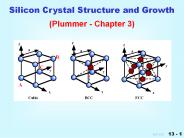
Silicon Crystal Structure and Growth ... mobile electrons tend ... Wafer positioning stage Three-axis piezo substage Figure 7.16 Detector Pinhole ...
| PowerPoint PPT presentation | free to download

FINISHING AND POLISHING The surface of the casting that is retrieved from investment is too rough for use in the mouth.Five preparatory procedures need to be ...
| PowerPoint PPT presentation | free to download

Increasing adoption of electric and hybrid vehicles and introduction of new technologies in automotive sector are key factors driving market growth.
| PowerPoint PPT presentation | free to download
Electrical symmetry destroyed by strain. Four energy valleys go down in energy, two go up (in biaxal strain) Vice versa in unaxial ...
| PowerPoint PPT presentation | free to download

Title: Brief Silicone Chemistry Review & Silicones for the Skin Care Industry Subject: Ken Kasprzak Author: Sherrie Wegener Last modified by: Wei You
| PowerPoint PPT presentation | free to view

A newly published report by Market Statsville Group (MSG), titled Global Thin Wafer Market provides an exhaustive analysis of significant industry insights and historical and projected global market figures. MSG expects the global Thin Wafer market will showcase an impressive CAGR from 2024 to 2033.
| PowerPoint PPT presentation | free to download

Companyprofilesandconferences.com glad to promote a new report on "Sino-American Silicon Products Inc.- Alternative Energy - Deals and Alliances Profile" which provides silicon products, solar products and oxide single crystal products. In addition, the company offers Antimony-doped wafers and Arsenic-doped wafers.
| PowerPoint PPT presentation | free to download

Bab 2 : Pembuatan Wafer 2.1 Struktur bahan Terdapat 3 struktur bahan yang berbeza Hablur tunggal Atom disusun di dalam ulangan corak yang sama Mempunyai sifat2 yg ...
| PowerPoint PPT presentation | free to view

Photograph courtesy of Kayex Corp., 300 mm Si ingot. Photo 4.1. EE-452 ... Developmental Specifications for 300-mm Wafer Dimensions and Orientation. Table 4.4 ...
| PowerPoint PPT presentation | free to view

CRYSTAL GROWTH, WAFER FABRICATION AND BASIC PROPERTIES OF Si WAFERS- Chapter 3 Crystal Structure Crystals are characterized by a unit cell which repeats in the
| PowerPoint PPT presentation | free to view

Chemical Polishing Slurry market has developed for several decades, and currently the global market is still dominated by few manufacturers from United States and Japan. Cabot Microelectronics is the largest producer, occupies for over 33 percent market share in the world, with manufacturing factories in US, Japan and Taiwan. The second-tier players are Hitachi Chemical, Fujimi Incorporated, Fujifilm, Dow Electronic Materials and Air Products/Versum Materials. The top six players occupy for over 88% market share.
| PowerPoint PPT presentation | free to download

Solar Cell Chapter 7: Manufacturing Silicon Solar Cells Nji Raden Poespawati Department of Electrical Engineering Faculty of Engineering University of Indonesia
| PowerPoint PPT presentation | free to view

Material preparation is the beginning of the process in making an IC chip. ... antimony and melted at 1400 in a quartz crucible surrounded by an inert gas ...
| PowerPoint PPT presentation | free to view

Solar Cell Chapter 7: Manufacturing Silicon Solar Cells Nji Raden Poespawati Department of Electrical Engineering Faculty of Engineering University of Indonesia
| PowerPoint PPT presentation | free to view

The global impacts of the coronavirus disease 2019 (COVID-19) are already starting to be felt, and will significantly affect the Polishing Slurry market in 2020.
| PowerPoint PPT presentation | free to download

Investigation of the Effects of the Wafer-Pad Contact Mode on CMP Performance SFR Workshop November 8, 1999 Yongsik Moon, Andrew Chang, Jianfeng Luo,
| PowerPoint PPT presentation | free to download

Elemental silicon is melted and grown into a single crystal ingot Single crystal ingot being grown Completed silicon ingot Pure silicon is rarely grown Typically as ...
| PowerPoint PPT presentation | free to download

SAND TO SILICON CHIPS. SAND TO SILICON CHIP. PATTERNING Si WAFERS FOR CHIP MANUFACTURING THE BILLION DOLLAR MICROFABRICATION WAY ...
| PowerPoint PPT presentation | free to view

Wafers are monocrystals from silicon, mainly made for microelectronic device ... Tribology, hard coatings. Packaging for food. Sensors and Measurement Systems ...
| PowerPoint PPT presentation | free to view

Grayscale technology is used to fabricate 3-D wedges ... Small chip size, lower cost due to batch silicon wafer fabrication in MEMS devices ...
| PowerPoint PPT presentation | free to view

Etching is done either in 'dry' or 'wet' methods ... Use oxidant to oxidize silicon to form silicon dioxide followed by HF etch of silicon dioxide ...
| PowerPoint PPT presentation | free to view

Estimation of Etch Depth for Blanket Wafers. Estimation for Patterned Wafers ... Pre-etch thickness measured using a Spectral Photometer. Accuracy /- 20 ...
| PowerPoint PPT presentation | free to view

Paula Collins, CERN Alan Honma, CERN Christian Joram, CERN Michael Moll, CERN Steve Worm, RAL Outline Why Silicon ? Semiconductor Basics Band-gap, PN junction Silicon ...
| PowerPoint PPT presentation | free to download

Speciality Materials. Main Products (in % of Total Sales) ... Speciality Products; Silicon Metals and Ferrosilicon (27 %) Aluminium billets and ingots (11 ...
| PowerPoint PPT presentation | free to download

Electrical Characteristics. Configuration Building Blocks. Switching Circuitry ... Enhancement vs Depletion mode devices ... All the devices on the wafer are ...
| PowerPoint PPT presentation | free to view

IC Fabrication and ... from a dopant-containing ambient or doped solid source Formation of Insulating Films The favored insulator is pure silicon ...
| PowerPoint PPT presentation | free to download

Front lithography/back Ohmic contact. Electrochemical etching. Back etching/polishing ... AFM lithography in constant current mode ...
| PowerPoint PPT presentation | free to view

EE 4345 - Semiconductor Electronics Design Project Silicon Manufacturing Group Members Young Soon Song Nghia Nguyen Kei Wong Eyad Fanous Hanna Kim Steven Hsu
| PowerPoint PPT presentation | free to view