Photoresists PowerPoint PPT Presentations
All Time
Recommended
Title: CMP Modeling Author: Terry A. Ring Last modified by: tring Created Date: 12/6/2000 2:11:46 AM Document presentation format: On-screen Show Company
| PowerPoint PPT presentation | free to download
Lecture 10.0 Photoresists/Coating/Lithography Semiconductor Fab Land $0.05 Billion Building $0.15 Billion Tools & Equipment $1 Billion Air/Gas Handling Sys $0.2 ...
| PowerPoint PPT presentation | free to download
photolithography to produce integrated circuits. What is photoresists. Photopolymers are imaging compositions based on polymers/oligomers/monomers ...
| PowerPoint PPT presentation | free to view
2014 Deep Research Report on Global LCD Photoresists Industry @ http://www.reportsnreports.com/reports/298088-2014-deep-research-report-on-global-lcd-photoresists-industry.html .
| PowerPoint PPT presentation | free to download
Added steric. bulk may restrict. rotation. New comonomers: ... new norbornene monomers with increased steric bulk to make hydrogenated polymer ...
| PowerPoint PPT presentation | free to download
Explore the Semiconductor Chemicals Market with our comprehensive analysis, unveiling the latest trends in chemicals and materials crucial for semiconductor manufacturing. From advanced photoresists to cutting-edge etchants, delve into market dynamics, key players, and emerging opportunities.
| PowerPoint PPT presentation | free to download
Photolithography Outline Motivation History Photolithography Methods and Theories Preparation and Priming Spin-Coating Photoresists Soft-baking Mask Alignment and ...
| PowerPoint PPT presentation | free to download
The market for imaging chemicals photoresists, developers, strippers, and ... In any optical imaging system, the size of the smallest element that can be ...
| PowerPoint PPT presentation | free to download
... 5Clariant Corporation Synthesis and Properties of Noval Fluoropolymer for 157nm Photoresists by Cyclo-polymerization Osamu Yokokoji1, Shun-ichi Kodama1 ...
| PowerPoint PPT presentation | free to view
Photoresist stripping equipment is used to remove the residuals of photoresists from silicon wafer after it is etched during the semiconductor chip fabrication process. The equipment plays an important role in the chip fabrication process in ensuring that the silicon wafers are free from impurities.
| PowerPoint PPT presentation | free to download
Photoresist stripping equipment is used to remove the residuals of photoresists from silicon wafer after it is etched during the semiconductor chip fabrication process. The equipment plays an important role in the chip fabrication process in ensuring that the silicon wafers are free from impurities.The analysts forecast global semiconductor photoresist stripping market to grow at a CAGR of 3.13% during the period 2016-2020.Complete Report available at http://www.sandlerresearch.org/global-semiconductor-photoresist-stripping-market-2016-2020.html.
According to the latest research report by IMARC Group, The Vietnam semiconductor materials market size reached US$ 4.4 Billion in 2023. Looking forward, IMARC Group expects the market to reach US$ 11.5 Billion by 2032, exhibiting a growth rate (CAGR) of 11% during 2024-2032. More Info:- https://www.imarcgroup.com/vietnam-semiconductor-materials-market
| PowerPoint PPT presentation | free to download
* * * * * * * * * Photolithographic Process J. Phys. Org. Chem. 2000, 13, 767. Coat Exposure Develop Strip Etch Photoresist Substrate Mask h Positive Negative ...
| PowerPoint PPT presentation | free to view
Photoresist physical properties. Applications of conventional i-line photoresist. ... Post-Exposure Bake. Required for Deep UV Resists ...
| PowerPoint PPT presentation | free to view
According to the latest research report by IMARC Group, The India semiconductor materials market size reached US$ 4.5 Billion in 2022. Looking forward, IMARC Group expects the market to reach US$ 6.5 Billion by 2028, exhibiting a growth rate (CAGR) of 6.3% during 2023-2028. More Info:- https://www.imarcgroup.com/india-semiconductor-materials-market
| PowerPoint PPT presentation | free to download
From MEMS to NEMS with Carbon
| PowerPoint PPT presentation | free to view
Big Market Research: “Photoresist Market 2019“Size, Share, Industry Trends, Demand, Insights, Analysis, Research, Report, Opportunities, Company Profiles, Forecast
| PowerPoint PPT presentation | free to download
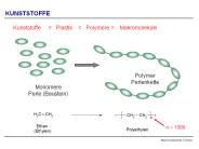
KUNSTSTOFFE Kunststoffe = Polymere Makromolek le = Plastik = Polymer Perlenkette Monomere Perle (Baustein) n 1000 Makromolekulare Chemie Makromolekulare Chemie DIE ...
| PowerPoint PPT presentation | free to download
Philips Thru Via Imaging Philips Thru Via Imaging Quadruple leads in a single through-wafer hole and a toroid structure Exposure Using Phase Gratings Schematic ...
| PowerPoint PPT presentation | free to download
Working mask set Pattern on wafers. Increasing device density reducing minimum feature size ... Reticle masks. 5-20. Working masks. 1. Optical or e-beam writing ...
| PowerPoint PPT presentation | free to view
Photolithography D. Boolchandani Department of ECE Malaviya National Institute of Technology
| PowerPoint PPT presentation | free to download
[226 Slides Report] Electronic Chemicals & Materials Market report categorizes the Global market by Types (Silicon Wafer, PCB Laminate, Photoresist, and Specialty Gases), Application (Semiconductor & IC, PCB), Forms (Solid, Liquid, and Gaseous) & Geography
| PowerPoint PPT presentation | free to download
Reduce charges since they degrade device operation T , H2 anneal. ... Oxide Charges and Their Annealing. Much more important in Si devices than in MEMS. Plummer et al. ...
| PowerPoint PPT presentation | free to view
[226 Slides Report] Electronic Chemicals & Materials Market report categorizes the Global market by Types (Silicon Wafer, PCB Laminate, Photoresist, Specialty Gases), Application (Semiconductor & IC, PCB), Forms (Solid, Liquid, Gaseous) & Geography
| PowerPoint PPT presentation | free to download
[226 Slides Report] Electronic Chemicals & Materials Market report categorizes the Global market by Types (Silicon Wafer, PCB Laminate, Photoresist, and Specialty Gases), Application (Semiconductor & IC, PCB), Forms (Solid, Liquid, Gaseous) & Geography
| PowerPoint PPT presentation | free to download
EE 4345 - Semiconductor Electronics Design Project Silicon Manufacturing Group Members Young Soon Song Nghia Nguyen Kei Wong Eyad Fanous Hanna Kim Steven Hsu
| PowerPoint PPT presentation | free to view
Developing. Hard-baking. References. Motivation. Key top-down ... Photomask is a square glass plate with a patterned emulsion of metal film on one side ...
| PowerPoint PPT presentation | free to download
During PEB, photo-acid diffusion causes amplification in a catalytic reaction ... Scanning Projection System. Synchronized mask and wafer movement. Slit. Lens ...
| PowerPoint PPT presentation | free to view
Title: Slide 1 Author: Chuck Fraust Last modified by: sfharper Created Date: 4/6/2004 9:13:43 PM Document presentation format: On-screen Show Company
| PowerPoint PPT presentation | free to download
NIST Advanced Embedded Passives Technology (AEPT) consortium test boards. ... Emulates existing high-speed board with buried components. ...
| PowerPoint PPT presentation | free to view
RESISTANCE TEMPERATURE DETECTOR (RTD) PROJECT Dr. Hisham E. Hegab College of Engineering & Science Louisiana Tech University Ruston, LA hhegab@latech.edu
| PowerPoint PPT presentation | free to view
Lithography Lithography in the MEMS context is typically the transfer of a pattern to a photosensitive material by selective exposure to a radiation source such as light.
| PowerPoint PPT presentation | free to download
The World Leader in High-Performance Signal Processing Solutions ... Hazardous wastes are generated from the many types of semiconductor manufacturing processes. ...
| PowerPoint PPT presentation | free to view
A Comparison of Resist Selectivity
| PowerPoint PPT presentation | free to view
Title: VI-6 Transfert image par r sine photosensible Photoresist imaging Author: Michel VERNET Last modified by: Michel VERNET Created Date: 8/8/2001 2:07:24 PM
| PowerPoint PPT presentation | free to download
VLSI Design Introduction Introduction Integrated circuits: many transistors on one chip. Very Large Scale Integration (VLSI) Complementary Metal Oxide Semiconductor ...
| PowerPoint PPT presentation | free to view
A Comparison of Resist Selectivity
| PowerPoint PPT presentation | free to view
Less than a decade ago, a typical circuit simulator would run only on mainframe computers. ... Process Conditions. Flow Rate: 20 to 50 liters/min. Time: 18 to 24 hours ...
| PowerPoint PPT presentation | free to view
Circuits DF-TM et MC m thode 'pattern plating ' DS-PTH & ML PCBs pattern plating method ... Titration du carbonate de soude. Avec HCl 0,1 N. Indicateur : m thyle ...
| PowerPoint PPT presentation | free to view
Micro-Electro-Mechanical Systems (MEMS) Submitted to: Mr.Deepak Basandari Made By: Rupesh Kumar
| PowerPoint PPT presentation | free to view
Brigham Young University Microfabrication Group. Microfabrication Mentoring Environment ... Brigham Young University Microfabrication Group. MME ...
| PowerPoint PPT presentation | free to view
Cross sectional view of a conventional double-tank cell ... Intentionally oxidize PS. Isolate the internal surface by capping. Modify the internal surface ...
| PowerPoint PPT presentation | free to download
... for waste reduction, recycling, and buying recycled products ... SIA collaborated with EPA to publish a comprehensive guide to Community Right-to-Know Reporting ...
| PowerPoint PPT presentation | free to view
... takes place when an impurity atom migrates to the vacancy or interstitial defect. ... movie. S32. For an intrinsic material, the diffusivity is given by: ...
| PowerPoint PPT presentation | free to view
Semiconductor Memory Design (SRAM & DRAM) Kaushik Saha Contact: kaushik.saha@st.com, mobile-98110-64398 Understanding the Memory Trade The memory market is the most ...
| PowerPoint PPT presentation | free to view
LITHOGRAPHY Chapter 5 in the Text
| PowerPoint PPT presentation | free to view
Photoresist And Photoresist Ancillaries Market
| PowerPoint PPT presentation | free to download
Global electrical and electronics materials market size is expected to reach $4.28 Bn by 2028 at a rate of 11.0%, segmented as by product, silicon wafer, pcb laminate, photoresist, other products
| PowerPoint PPT presentation | free to download
The global photoresist and photoresist ancillaries market size grew from $3.54 billion in 2022 to $3.88 billion in 2023 at a compound annual growth rate (CAGR) of 9.5%.
| PowerPoint PPT presentation | free to download
Photoresist & Photoresist Ancillaries Global Market Report 2022 By The Business Research Company
| PowerPoint PPT presentation | free to download
TBRCs global photoresist & photoresist ancillaries market report includes arf immersion, krf, arf dry, g- and i-line, anti-reflective coatings, remover, developer https://bit.ly/3ChoP1a
| PowerPoint PPT presentation | free to download
Download Free Research Report PDF: http://bit.ly/2qyPFSQ #PhotoresistChemicalsMarket #MarketAnalysis According to this study, over the next five years the Photoresist Chemicals market will register a 4.8% CAGR in terms of revenue, the global market size will reach US$ 3787.2 million by 2024, from US$ 2998.3 million in 2019. Full Report Url: http://bit.ly/2CmCVBh
| PowerPoint PPT presentation | free to download
Major players in the photoresist & photoresist ancillaries market are Tokyo Ohka Kogyo Co. Ltd., JSR Corporation, DuPont, Shin-Etsu Chemical Co. Ltd., Sumitomo Chemical Co. Ltd., Fujifilm Electronic Materials, Merck KGaA, Allresist GmbH. Read more @ https://bit.ly/3AzP7dU
| PowerPoint PPT presentation | free to download
Download Free Research Report PDF : http://bit.ly/2mpO1kg #Photoresist #MarketAnalysis Photoresist market was valued at USD XX million globally in 2018 and is forecasted to reach USD XX million by 2024, with a CAGR of xx% during the 2018-2024. Full report Url : http://bit.ly/2lX9Szg
| PowerPoint PPT presentation | free to download
Download free PDF Sample: https://bit.ly/2VpGpwD #LiquidPhotoresist #MarketAnalysis The global Liquid Photoresist market size is expected to gain market growth in the forecast period of 2020 to 2025, with a CAGR of xx%% in the forecast period of 2020 to 2025 and will expected to reach USD xx million by 2025, from USD xx million in 2019.
| PowerPoint PPT presentation | free to download
The research report has incorporated the analysis of different factors that augment the market?s growth. It constitutes trends, restraints, and drivers that transform the market in either a positive or negative manner. This section also provides the scope of different segments and applications that can potentially influence the market in the future. The detailed information is based on current trends and historic milestones.
| PowerPoint PPT presentation | free to download


