Multi-functional Packaged Antennas for Next-Generation Wireless Applications - PowerPoint PPT Presentation
1 / 8
Title:
Multi-functional Packaged Antennas for Next-Generation Wireless Applications
Description:
The reverse biased p-n junction results in zero drain current. ... Note that the BJT and MOSFET are both back-to-back p-n diodes, ... – PowerPoint PPT presentation
Number of Views:56
Avg rating:3.0/5.0
Title: Multi-functional Packaged Antennas for Next-Generation Wireless Applications
1
Operation in the Cutoff Region
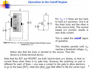
For VGS 0 there are two back to back p-n
junctions. One is at the drain body and the other
is at the source body. The reverse biased p-n
junction results in zero drain current. This is
called the cutoff region of operation. This
situation persists until VGS reaches a threshold
voltage, Vt0.
Notice also that the body is shorted to the
source. Thus the device is a three terminal
device.
Note that the BJT and MOSFET are both
back-to-back p-n diodes, so that no current flows
when there is no gate bias. However, the
switching on part is different for each of them
one uses a contact to the gate to allow electrons
to go to the base (BJT), while the other uses
field effect to flip the carrier type in the base
to produce conduction (MOSFET).
2
Operation in the Triode Region
For VGS gt Vt0, the electric field resulting from
the gate voltage repels holes from the region
under the gate, but attracts electrons, which can
now flow easily between two n-type contacts
(drain and source). This phenomenon manifests
itself as an n-type channel between the drain and
the source (thus the name n-MOS). Thus when
positive VDS is applied current flows into the
drain, through the channel, and out of the
source. For small values of VDS the drain
current, iD is proportional to VDS. iD is also
proportional to VGS Vt0. This called the Triode
Region.
3
Operation in the Triode Region contd.
In the triode region, the NMOS device behaves as
a resistor connected between the source and the
drain. The resistance decreases as VGS increases.
Thus, FETs are sometimes used as voltage
controlled resistors. For instance, for an
amplifier, in which the gain depends on a certain
resistance value we can control the gain by using
a FET. The FET will provide variable resistance
and hence can be used for automatic gain control
(AGC).
4
Operation in the Saturation Region
As VDS continues to increase the uniform channel
starts to taper off in the direction of the
drain. This is due to increase in electric field
in that region. The consequence is higher channel
resistance and an almost constant drain current
after the VDS becomes larger than VGS - Vt0 .
This region is called the saturation region of
the NMOS. In summary For VDS lt VGS-Vt0 Triode
region For VDS VGS-Vt0 Saturation region
5
Expression of drain current in the Triode Region
6
Operation in the Saturation Region
Fig. 5.6 Characteristic curves for an NMOS
transistor
Note that the different characteristics are a
function of voltage, not current, unlike BJTs
Since at the boundary VDS VGSVt0, we have the
drain current given as
7
Example 5.1
8
The sinusoid signal will be distorted if the ac
input signal is large. However, the distortion
can be neglected if the signal is small.


