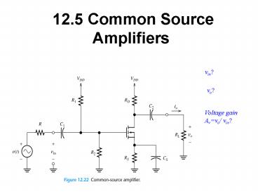
12.5 Common Source Amplifiers
1 / 15
Title: 12.5 Common Source Amplifiers
1
12.5 Common Source Amplifiers
vin?
vo?
Voltage gain Avvo/ vin?
2
Common-Source Amplifiers
- C1 and C2 are coupling capacitors and Cs is the
bypass capacitor. The capacitors are intended to
have large impedances for the dc signal and very
small impedances for the ac signal.
3
Common-Source Amplifiers
- For DC analysis, the capacitors are replaced by
open circuits to determine the quiescent
operation point (Q point). The transconductance
gm for the small-signal equivalent circuit is
also determined. - For AC analysis, the capacitor are replaced by
short circuits to determine the ac voltage gain
Avvo/vin.
4
DC Analysis
DC voltage sources
Coupling capacitors
Bypass capacitors
5
The Small-Signal Equivalent Circuit
- In small-signal midband analysis of FET
amplifiers, the coupling capacitors, bypass
capacitors, and dc voltage sources are replaced
by short circuits. - The FET is replaced with its small-signal
equivalent circuit. Then, we write circuit
equations and derive useful expressions for
gains, input impedance, and output impedance.
6
AC Analysis
DC voltage sources
Coupling capacitors
Bypass capacitors
7
DC voltage sources
Coupling capacitors
Bypass capacitors
8
SMALL-SIGNAL EQUIVALENT CIRCUITS (12.4)
A more complex equivalent circuit consider drain
resistance rd
9
Common Source Amplifiers FET source ??ground
10
Common Source Amplifiers
Equivalent load resistance
Input voltage output voltage
Voltage Gain
11
Common Source Amplifiers
Input Resistance
- Output resistance
- disconnect the load,
- replace the signal source by
- the internal resistance,
- find the resistance by looking
- into the output terminals.
12
Example 12.4
Analyze the following circuit. KP50uA/V2, Vto2
V, L10um, W400um (identical to example 12.2).
- Assume
- Find
- midband voltage gain
- input resistance
- output resistance
- output voltage
13
Example 12.4
Analyze the following circuit. KP50uA/V2, Vto2
V, L10um, W400um (identical to example 12.2).
DC Analysis Fine Q point (see example 12.2)
14
Example 12.4
Analyze the following circuit. KP50uA/V2, Vto2
V, L10um, W400um (identical to example 12.2).
AC Analysis Fine gm(see Ch 12.4)
Equivalent load resistance
Voltage Gain
15
Example 12.4
Analyze the following circuit. KP50uA/V2, Vto2
V, L10um, W400um (identical to example 12.2).
Input Resistance
Output Resistance
Input voltage
Output voltage


