Chip v4: - PowerPoint PPT Presentation
1 / 1
Title:
Chip v4:
Description:
Physic experiment : A near ... 20.27 20.27 20.27 20.27 20.27 20.27 20.27 20.27 20.27 7.08 4.80 5.04 5.80 7.13 7.10 7.60 8.70 9.40 186.00 187.00 192.00 212.00 245.00 ... – PowerPoint PPT presentation
Number of Views:34
Avg rating:3.0/5.0
Title: Chip v4:
1
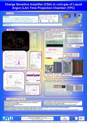
Charge Sensitive Amplifier (CSA) in cold gas of
Liquid Argon (LAr) Time Projection Chamber (TPC)
- Context
- Specifications
- Multichannel 3fC to 120fC (0.5µs pulse) Charge
Sensitive Amplifier - Less than 1500 e- ENC with 250pF Detector
capacitance (Signal/Noise ratio of 10) - Able to work in LAr vapours _at_ -150C with an
affordable power dissipation 1mW/channel,
considering a power pulsing rate of 2.5
(effective consumption 40mW) - Low cost highly integrated solution implies an
ASIC CMOS process circuit.
- Physic experiment
- A near detector (from the Hardron target) will
allows physic experiments as well as electronic
experiments for larger scale detectors (100
kilotonnes )
- 4 chips comparison
- Noise
- Version 1 detailed in 1 has no integrated
shaper. With an external shaper, noise reaches
1100 e- at -110C. - Version 2 has a default in the amplifier of the
shaper. A re-design was necessary. - Version 3 Modified CSA using Gain Boost
technique2. Stability issue due to a bad sizing
of the compensation resistance. Results higher
noise at low temperature - Version 4 is range limited because the intrinsic
gain had been voluntary increased
Noise summary
OUT_PA-noise Device Param Noise
Contribution Of Total /MP34 id
0.000417014 32.85 /MN8
id 0.000292864 16.20 /MN8
fn 0.000186043 6.54
/MN180 id 0.000185096
6.47 /MN19 id
0.000155535 4.57 /MN180 fn
0.000144948 3.97 /MP36 id
0.000129472 3.17 /R1/R2
thermal_noise 0.000128369 3.11
/R1/R1 thermal_noise 0.000128365
3.11 /R27 rn
0.00012745 3.07 /MN33 id
0.000112945 2.41 /MP1 id
0.000109437 2.26 /MP2
id 0.000101267 1.94 /MN19
fn 8.17541e-05 1.26
/MP33 id 8.03967e-05
1.22 /R5 rn
7.19811e-05 0.98 /MP123 id
6.79982e-05 0.87 R6.R2.rpolyh1
thermal_noise 6.73008e-05 0.86 /MP35
id 6.48913e-05 0.80
/MP34 fn 5.46878e-05
0.56 R6.R1.rpolyh1 thermal_noise
5.10705e-05 0.49 /MN32 id
5.08948e-05 0.49 R3.R2.rpolyh1
thermal_noise 4.92785e-05 0.46
R3.R1.rpolyh1 thermal_noise 4.25442e-05
0.34 R4.R1.rpolyh1 thermal_noise
4.15188e-05 0.33 R4.R2.rpolyh1
thermal_noise 3.98648e-05 0.30
R2.R1.rpolyh1 thermal_noise 3.98639e-05
0.30 R2.R2.rpolyh1 thermal_noise
3.97519e-05 0.30 /I10/MP1 id
3.08658e-05 0.18 Integrated Noise
Summary (in V) Sorted By Noise Contributors Total
Summarized Noise 0.000727636 Total Input
Referred Noise 0.493965
1
2
3
4
5
6
7
6
7
1
- Version 4 configurations
- Cpa 250 or 500fF
- Rpa 1, 2, 3 or 4MO
- Shaping center frequency 0.5, 1, 2 or 4 µs
5
2
3
4
- Chip v4
- Histograms measure of the noise could be
experimentally observed out of - the ADC with the DAQ system 3. The delta
5.4mV corresponds to FWHM/2 - (Full width at half maximum). Since the rms Noise
(s) FWHM/2.35 - We verify that "sqrt-integ-noise2" maximum
value 5.32 5.4mV2/2.35
- A Labview interface controls a DAQ-USB that
controls a clock, and a data frame. The slave
responds by pulling down the data-bus wire. - A 800-line vhdl file generates the 100µ x 550µ
I2C-like slave. The size could be adjusted when
more registers are needed.
- Chip v4
- Noise comparison
- of the CSA with
- ideal bias current (PA12)
- versus
- fully designed CSA (PA2)
- Fully digital I2C-like
- configuration protocol
CSA
Shaper
Buffer
- Chip v4
- MIP signal with oscilloscope persistence
- Experimental results of various versions chips.
- - First version noise is better since the shaper
was external. - - For the latest version, a noise reduction is
obtained by cooling - down the chip at the level of the actual detector
capacitance.
- Version 2 TOP_EST
- 1974µm X 2364µm
- 4.66mm²
- Version 1 PA_TOP
- 1654µm X 1664µm
- 2.75mm²
- Version 3 TOPPING
- 1914µm X 2544µm4.876mm²
- Version 4 T2K_V4
- 1914µm X 2684µm5.14mm²
- Experimental application
32-channel
- Chip v4
- Measurement from room temperature
- down to LN2.
8 channels x 4 chips 32 channels per pane. 3
pane in the LAr tank (vapours) one outside
- Application in a joint test with LHEP Bern
- Conclusion and Perspectives
- Evident difficulties of prototyping a circuit
without models at low temperature (-150C) - Improvement on the consumption at equal noise
level are under study. Effort on biasing element
could be profitable. - A low quiescent current buffer is under test.
- Specifications fulfilled.
- An investigation on the AMS 180nm will be done
when the technology will be available. - A 128-channel test (4 cards of 4 chips of 8
channels) on a detector with a digital
acquisition 3 system will be published rapidly. - When the design will be validated, a 32 or
64-channel chip will be submitted.
1 CMOS Charge amplifier for liquid argon Time
Projection Chamber detectors, E. Bechetoille,
WOLTE08, Jena, Germany. http//hal.in2p3.fr/in2p3-
00339737/ 2 Feedforward compensation techniques
for high-frequency CMOS amplifiers, W. Sansen,
3 MicroTCA implementation of synchronous
Ethernet-Based DAQ systems for large scale
experiments, C. Girerd et al. RT2009, Beijing,
China. http//hal.in2p3.fr/in2p3-00394783/
E.Bechetoille, H. Mathez, Y. Zoccarato IPNL, 4
rue E. Fermi 69622 Villeurbanne, France
University Lyon 1, CNRS/IN2P3, MICRhAu contact
e.bechetoille (at) ipnl.in2p3.fr
NSS-MIC 2010 - 2010 IEEE Nuclear Science
Symposium and Medical Imaging Conference -
Knoxville, Tennessee, 30 October 6 November
2010


