Experimental setup - PowerPoint PPT Presentation
1 / 12
Title:
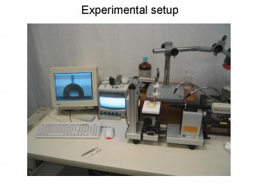
Experimental setup
Description:
nitride not as tight as LPCVD, deposition sensitive to dust particles. deposition temp. ... high deposition temperature, nitride always needed (Na ... – PowerPoint PPT presentation
Number of Views:111
Avg rating:3.0/5.0
Title: Experimental setup
1
Experimental setup
2
Sample holders / clamping
3
Video setup / wiring
4
Electrowetting / basics
- Important properies
- low leakage current
- high ?r
- high contact angle
- charge trapping behaviour ?
5
Tested film combinations
6
PECVD teflon-like coating13.56MHz
parallel-plate RIE, CHF3 / CF4 plasma
7
Electrowetting experiment / DI-waterSi substrate
/ 250nm PECVD SixNy / 20nm PECVD SixOy / 10nm FC
8
Electrowetting experiment / NaCl water sol.Si
substrate / 250nm PECVD SixNy / 20nm PECVD SixOy
/ 10nm FC
9
Electrowetting experiment / charge trappingSi
substrate / 150nm LPCVD SixOy / 350nm LPCVD SixNy
/ 10nm FC
10
Electrowetting experiment / 2-waferBottom Si
substrate / 10nm FCTop Si substrate / 250nm
PECVD SixNy / 20nm PECVD SixOy / 10nm FC
11
Electrowetting experiment / breakthroughTiny
defect great troubles
12
Conclusions
- Video setup was upgraded extended
- Best film combination so far SixNy/SixOy/CF
- Both single wafer and 2-wafer configuration
succesfully tested - Charge trapping effect ( bipolar behaviour)
observed - Behaviour depends on ion concentration
- Detailed analysis of the trapping effect needed
(transient current characteristics with and w/o
liquid, XPS, AFM ) - Control electronics has to be integrated into the
setup, on-screen status display needed - Patterned structures ? nitride step coverage


