CCID20 General Characteristics - PowerPoint PPT Presentation
1 / 14
Title:
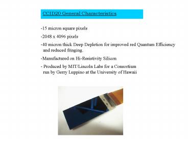
CCID20 General Characteristics
Description:
... very thin crystalline layer of Boron doped Silicon on the CCD ... Layer of Boron doped Silicon (This chip had a blue optimised Anti-reflection. coating. ... – PowerPoint PPT presentation
Number of Views:41
Avg rating:3.0/5.0
Title: CCID20 General Characteristics
1
CCID20 General Characteristics
-15 micron square pixels -2048 x 4096
pixels -40 micron thick Deep Depletion for
improved red Quantum Efficiency and reduced
fringing. -Manufactured on Hi-Resistivity
Silicon - Produced by MIT/Lincoln Labs for a
Consortium run by Gerry Luppino at the
University of Hawaii
2
ESO/AAO TEST DATA ON CCID20
Noise
Point Spread Function
Fringing
None visible at 950nm
Cosmic Rays
3000 events per hour. Similar to a standard
thinned CCD. Each event, however, will affect
more pixels than for a normal thinned CCD.
3
Physical Configuration of CCID20 Camera
The optical distance from the front surface of
the cryostat to the chip surface will be about
12mm. When mounted on ISIS RED the long axis of
the chip will be horizontal.
4
Physical Configuration of CCID20 Camera
5
CCID20 Mosaic Camera
Subsequent CCID20 devices will be mounted in a
2-chip mosaic
6
Charge Collection in a CCD.
Photons entering the CCD create electron-hole
pairs. The electrons are then attracted towards
the most positive potential in the device where
they create charge packets. Each packet
corresponds to one pixel
pixel boundary
pixel boundary
incoming photons
Electrode Structure
Charge packet
SiO2 Insulating layer
7
Deep Depletion CCDs 1.
The electric field structure in a CCD defines to
a large degree its Quantum Efficiency (QE).
Consider first a thick frontside illuminated CCD,
which has a poor QE.
Cross section through a thick frontside
illuminated CCD
In this region the electric potential gradient
is fairly low i.e. the electric field is low.
Any photo-electrons created in the region of low
electric field stand a much higher chance of
recombination and loss. There is only a weak
external field to sweep apart the
photo-electron and the hole it leaves behind.
8
Deep Depletion CCDs 2.
In a thinned CCD , the field free region is
simply etched away.
Cross section through a thinned CCD
Electric potential
Electric potential
There is now a high electric field throughout the
full depth of the CCD.
Problem
Thinned CCDs may have good blue response but
they become transparent at longer wavelengths
the red response suffers.
This volume is etched away during manufacture
Red photons can now pass right through the CCD.
Photo-electrons created anywhere throughout the
depth of the device will now be detected.
Thinning is normally essential with backside
illuminated CCDs if good blue response is
required. Most blue photo-electrons are created
within a few nanometers of the surface and if
this region is field free, there will be no blue
response.
9
Deep Depletion CCDs 3.
Ideally we require all the benefits of a thinned
CCD plus an improved red response. The solution
is to use a CCD with an intermediate thickness
of about 40mm constructed from Hi-Resistivity
silicon. The increased thickness makes the
device opaque to red photons. The use of
Hi-Resistivity silicon means that there are no
field free regions despite the greater thickness.
Cross section through a Deep Depletion CCD
Electric potential
Electric potential
Problem
Hi resistivity silicon contains much lower
impurity levels than normal. Very few
wafer fabrication factories commonly use
this material and deep depletion CCDs have to be
designed and made to order.
Red photons are now absorbed in the thicker bulk
of the device.
There is now a high electric field throughout the
full depth of the CCD. CCDs manufactured in this
way are known as Deep depletion CCDs. The name
implies that the region of high electric field,
also known as the depletion zone extends
deeply into the device.
10
BIV Process.
The design shown here and on the previous page is
the basic BIV process. The surface of the chip
is actually left with a thin coating of Silicon
Dioxide which modifies the electric field in the
first few nanometers of the CCD producing a trap
for photo-electrons created in this area. The
chip therefore has a poor blue QE.
Electric potential
Electric potential
Red photons penetrate deeply
Blue photons absorbed at surface
11
MBE Process
The Molecular Beam Epitaxy (MBE) process will be
added to some of the BIV devices to recover the
blue response. The MBE process involves laying
down a very thin crystalline layer of Boron doped
Silicon on the CCD surface. This creates a built
in -ve potential at the CCD surface that repels
any photo-electrons created at the surface and
allows them to be collected in the potential
well of the nearest pixel.
Electric potential
Electric potential
(This chip had a blue optimised
Anti-reflection coating. The final devices will
have broad band coatings that will further
enhance the red response)
Layer of Boron doped Silicon
12
Comparison with existing OASIS CCDs
13
Alternative Red Sensitive CCDs
14
CCID20 Deep Depletion CCD Delivery
- Five BIV wafers have left the wafer fab and are
currently being processed. From these the - University of Hawaii has received 4 device
only one of which is Science grade, two others - being unusable due to charge spreading, and the
fourth is cosmetically very poor. - University of Hawaii also expects to receive
some MBE devices at the end of the summer. - Gerry Luppinos estimate is that we will receive
our first Science chip by the end of the year. - He has offered us the above mentioned
cosmetically poor chip as an engineering
sample.


