Introduction and Motivation - PowerPoint PPT Presentation
1 / 1
Title: Introduction and Motivation
1
Optical Interconnects Optimal Etching
Conditions for the Fabrication of Channel
Waveguides
Navnit Agarwal, Shom Ponoth, Joel Plawsky,
Peter Persans Department of Electrical,
Computer and Systems Engineering, Department of
Chemical Engineering, Department of
Physics Rensselaer Polytechnic Institute, Troy NY
Ph (518) 276-6032 Fax (518) 276-8761 Email
agarwn_at_rpi.edu
- Introduction and Motivation
- Waveguided interconnects are one possible
approach towards implementing optical
interconnects for on-chip and off-chip
applications - Desirable optical properties include low losses
and high index difference (between core and
cladding) for increased scalability - High index difference coupled with roughness at
the core-cladding interface can increase
scattering losses in the waveguide and impediment
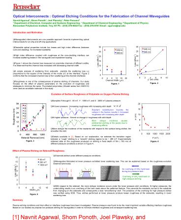
scaling - Figure 1 shows the channel loss measured on
polyimide channels of different widths. It is
observed that the channel loss increases with
decreasing channel width. - A simple analysis of scattering from sidewalls
predicts the scattering loss (a) proportional to
the square of the intensity of the mode (f2) at
the interface. Figure 2 confirms that the
increased channel loss is from scattering at the
channel interfaces - Roughness is one of the consequences of plasma
etching of channels. Our study focuses on the
effect of plasma parameters on the evolution of
roughness and strategies to minimize the same.
Fluorinated polyimides (Ultradel series from
AMOCO) were used as candidate materials in this
study
Figure. 2
Figure. 1
- Samples A through E 40 mT, F 1000 mT, and G
2000 mT plasma pressure - At lower pressure Increasing roughness with
increasing etch depth - At higher pressure Almost no change in
roughness with etch depth - More oblique the incidence of the reactants with
respect to the surface being etched, the smoother
the etch - Details available in 1. Based on our
explanation, we estimate the transition region
between a rough etching to a smooth etching
regime to be 465 mT. Experimentally obtained
data on the roughness produced on etching a fixed
depth of film ( 750 nm) at different pressure
conditions is shown in Figure 4.
Evolution of Surface Roughness of Polyimide on
Oxygen Plasma Etching
Reactant redistribution towards the valleys in
the feature results in increased roughness with
increasing etch depth
More oblique incidence causes preferential
etching at the peaks due to shadowing effects
Figure. 3
Figure. 4
- Channels etched under different pressure
conditions - Waveguides fabricated at lower pressure exhibited
lower scattering loss. This can be explained
based on the roughness evolution observed
previously. - With respect to the sidewall, the more oblique
incidence occurs under the lower pressure etch
conditions. At higher pressures, the undercutting
results in an overhang of the hard mask above the
patterned feature. This prevents the reactants
normal to the substrate from impinging on the
sidewalls and consequently a less smoothening
etch. The presence of the overhang for high
pressure etches was verified using SEM. Thus,
etches performed at lower pressure produce lesser
roughness at the sidewalls, resulting in lower
scattering loss.
Effect of Plasma Etching on Sidewall Roughness
No overhang of SiNx hardmask during low pressure
etch
Overhang of SiNx hardmask on high pressure
etching
Figure. 5
Summary Plasma etching conditions and their
effect on interface roughness have been
investigated. Plasma pressure was found to be the
most important variable effecting interface
roughness. Based on our studies we propose low
pressure etching for waveguides in order to
minimize interface roughness and consequent
scattering loss.
1 Navnit Agarwal, Shom Ponoth, Joel Plawsky,
and P. D. Persans, Applied Physics Letters, vol
78, no 16, pp 2294-2296, 2001


