AMCS group - PowerPoint PPT Presentation
1 / 1
Title:
AMCS group
Description:
Y.M. Galperin, P.E. Goa, and T.H. Johansen. This work is done with ... Experiments performed by P. E. Goa in Oslo, 2001. Develop a model for the domain wall. ... – PowerPoint PPT presentation
Number of Views:80
Avg rating:3.0/5.0
Title: AMCS group
1
How to Push Magnetic Vortices Around
UiO Dept. of Physics
FUNMAT NANOMAT
J.I. Vestgården, D.V. Shantsev, Å.A.F. Olsen,
V.V. Yurchenko, Y.M. Galperin, P.E. Goa, and
T.H. Johansen
AMCS group
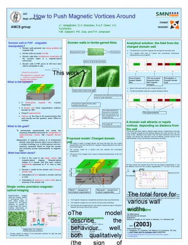
Domain wall in FGF - magnetic manipulator?
- Domain walls generate very strong gradients of
magnetic field - Domain walls are easily movable
- Domain walls allow simultaneous visualization of
the movable object in a magneto-optical
microscope - Domain walls in FGF grown at UiO have been used
to manipulate or trap - Ultracold neutral atoms
- DNA attached to a magnetic bead
- Vortices in superconductors
- Magneto-tactic bacteria
- Colloidal particles
This work
What is the system?
- A ferrite-garnet magnetic film, in-plane
magnetized - A domain wall where magnetization switches
direction by 180º. - A type-II superconductor
- Vortices, i.e. flux lines in the superconductor
that carry exactly one flux quantum, about 100nm
in diameter
What is the goal?
To demonstrate experimentally and create the
necessary theoretical framework for manipulation
of superconducting vortices with magnetic domain
walls Manipulation of magnetic vortices is of
fundamental interest, since their discrete nature
can be utilized in a number of settings, e.g. in
(both quantum and non-quantum) computers based on
singe flux quanta and extremely precise
measurements of magnetic fields.
Proposed model Charged domain wall
- The model is called a charged domain wall since
the field from the in-plane magnetization looks
like the field from magnetic charges attached to
the side of the wall (see figure) - The common model for a domain wall only contains
the out-of-plane magnetization - The source of the charges is the in-plane
component perpendicular to the wall, i.e.
Msin(f).
Dipole - charges from out-of-plane
magnetization
Monopole charges from in-plane magnetization
- The magnetic charges are energetically expensive
(long rang interactions) - The magnetic charges can only exist for strong
in-plane anisotropy - We introduce the charged domain wall model to
explain the sign of interaction between the
domain wall and the vortices - The model describe the behaviour well, both
qualitatively (the sign of interaction) and
quantitatively (the excess vortex distribution)
More information The AMCS group http//www.fys
.uio.no/super Experiment P.E.Goa, H. Hauglin,
Å. A.F. Olsen, D. Shantsev, T. H. Johansen, APL
82(1) (2003) TheoryExperiment J.I.
Vestgården, D.V. Shantsev, Y.M. Galperin, V.V.
Yurchenko, P.E. Goa, Å.A.F. Olsen, and T.H.
Johansen, cond-mat/0607043
- Experimental parameters
- Superconductor NbSe2
- London penetration depth 70 nm 200 nm
- Critical temperature 7.2 K
- Temperature 4 K 7 K
- FGF (Bi,Lu)3(FeGa)5O12
- Magnetization 50 kA/m
- Film thickness 0.8 mm
- Film/SC gap 140 nm
- Wall width 400 nm 3 mm
- This work is done with financial support from
- The Norwegian Research Council and the NANOMAT
program - FUNMAT_at_UiO


