- PowerPoint PPT Presentation
1 / 10
Title:
Description:
Sputter Rippling : Surface Self-Organization during Ion Beam Erosion 750 eV Ar+ spatially uniform over ~1 cm (lab); 300 cm (industry) 0.2 to 0.7 mA/cm2 – PowerPoint PPT presentation
Number of Views:6
Avg rating:3.0/5.0
Title:
1
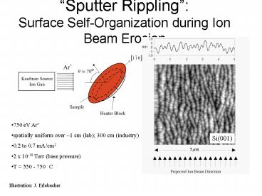
Sputter RipplingSurface Self-Organization
during Ion Beam Erosion
- 750 eV Ar
- spatially uniform over 1 cm (lab) 300 cm
(industry) - 0.2 to 0.7 mA/cm2
- 2 x 10⁻¹⁰ Torr (base pressure)
- T 550 - 750 C
Illustration J. Erlebacher
2
Occasional Uniformity
Slide courtesy of Bashkim Ziberi,
Leibniz-Institut für Oberflächenmodifizierung
Some images from Ziberi, Frost, Hoche,
Rauschenbach, PRB 72, 235310.
3
Sputter Rippling Tool?
Semiconductors
Metals
Cu(110) Rusponi, Constantini,Borragno,
Valbusa, PRL 81, 4184.
GaSb(001). Normal incidence ?Ordered arrays of
dots, sizes as small as 15 nm! Facsko et al.,
Science 285, 1551.
Insulators
- What might these be good for?
- Optical gratings on-chip photonics
- Specialized growth substrates
- Orienting liquid crystals, biopolymers, etc.
- Data-storage arrays
SiO2 Mayer, Chason, Howard, JAP 76, 1633.
- Fundamental science
- -nanoscale morphology evolution
- -ion-surface interactions
- surface energetics, kinetics
4
- Vertical templating for materials integration
5
outside patterned area
inside patterned area
cross-section of topography of original ridge
pattern
6
Origin of Characteristic Spacing
Roughening Rate (Sigmund)
Erosion at point x due to ions hitting at all
points x
P. Sigmund, J. Mater. Sci. 8, 1545 (1973).
7
(No Transcript)
8
Sputter Solitons?
Mg Alloy AZ91D IRRADIATION 30 keV Ga FIB normal
incidence Viewing angle 52
NEEDED Nonlinear physics of propagating edges
large slope changes
W. Zhou MJA (unpublished)
9
self-sharpening
shock front
10
Sputter Metastability
- FIB -gt Si(001)
- In-Situ Imaging
- 30 keV Ga
- Room Temp.
movie from SEM images
1 mm
W. Zhou MJA (unpublished)
11
1 keV Ne?Ag(001), STM, fromCostantini et al.
schematic cross section of crater formation on
single ion impact
100 keV Xe?Au(111), MD, from Bringa et al.
12
Figure 8 Fabrication procedure (a-f) for
micro-mold, soft-edged Occulter. In (a)-(f),
yellow material is sacrificial substrate black
is chromophore-bearing glass white is
chromophore-free glass. (a) Ion milling of pit
in sacrificial substrate using Focused Ion Beam
(b) filling with chromophore-bearing glass (c)
deposition of transparent handle (d), (e)
dissolution of sacrificial substrate (f)
deposition of chromophore-free glass.
Fig. 2. Fabrication procedure for direct-milled,
soft-edge Lyot stops. In (a), the absorbing
material (black)is deposited as a layer of known
thickness onto the substrate (light blue), (b)
then the mask shape(height function) is milled,
and (c) the mask is embedded in clear, dye-free
glass (also light blue).
Results from FIB manufacturing tests performed by
Shilpa N. Raja as part of a Harvard-DEAS Research
Experience for Undergraduate (REU) program (4).
The SEM-picture shows a direct-milled absorber
cone. The material is PMMA doped with Oilblack BT
dye.


