Motivation: Reactive Radio - PowerPoint PPT Presentation
1 / 9
Title:
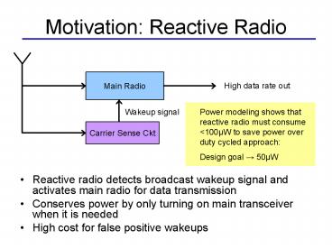
Motivation: Reactive Radio
Description:
... Reactive Radio. Reactive radio detects broadcast wakeup signal and activates main radio for data ... Conserves power by only turning on main transceiver ... – PowerPoint PPT presentation
Number of Views:64
Avg rating:3.0/5.0
Title: Motivation: Reactive Radio
1
Motivation Reactive Radio
Main Radio
High data rate out
Wakeup signal
Power modeling shows that reactive radio must
consume lt100µW to save power over duty cycled
approach Design goal ? 50µW
Carrier Sense Ckt
- Reactive radio detects broadcast wakeup signal
and activates main radio for data transmission - Conserves power by only turning on main
transceiver when it is needed - High cost for false positive wakeups
2
Digital Oscillator Calibration
- Calibrate LC oscillator with high accuracy
reference (FBAR) - Convert control voltage to digital signal and
control oscillator frequency digitally - Turn off FBAR oscillator and control loop after
calibration to save power. Control word from ADC
is latched while loop is off.
Low-accuracy LC oscillator (lt100µW)
To calibrate over 200MHz span better than 500kHz
accuracy, 400 steps (9 bits) required
9
FBAR osc
ADC
PD
LPF
.
.
.
High-accuracy (500ppm) FBAR oscillator (300µW)
3
Low Power Oscillator Strategies
- Subthreshold biasing
- greater transconductance (gm) for a given bias
current - device ft lower in subthreshold, but CMOS
scaling helps
- Low supply voltage
- CMOS supply is always shrinking
- previous oscillator work shows operation without
performance degradation down to 300mV supply
4
Oscillator Core
Vdd
- Vdd 500mV (or lower)
- Ibias 200µA
- f0 1.8 - 2.0GHz
- L 3nH (bondwire)
- Device W/L300/.13 (deep subthreshold regime)
- Fully differential output with 50O buffers
(500mVp-p) - Independent control of capacitor banks on each
output
off-chip
L
L
Nominal power consumption 100µW
Digitally controlled capacitor bank (0-511fF)
5
LSB Capacitor Design
- ?C1fF, Cunit20fF, N19
- Finger caps for good matching and Q
- Switch parasitics can be absorbed into array of N
caps - Form binary arrays of this basic unit for larger
caps
Cunit
Vctrl1
Cunit
Cunit
Cunit
N
2
1
6
MSB Capacitor Design
- ?C32fF, Cunit36fF
- Finger caps for good matching and Q
- Switch parasitics can NOT be absorbed into array
of caps - Form binary arrays of this basic unit for larger
caps
(5/.13)
1
Cunit
2
Cunit
(.15/1)
(.15/1)
N
Vctrl1
7
Capacitor Bank Segmentation
Simulation results Bit 1? ?f 410kHz Bit 2? ?f
830kHz
N-ratio scheme
Cunswitched 600fF
(extraction shows about 800fF with routing)
Single switched capacitance
Cunswitched 150fF
8
Effects of Segmentation Mismatch
Design for overlapping bands to maintain
frequency resolution
Cmsb lt 31 Clsb
- Overlapping bands, no missing codes
- Reduced tuning range
Alternative
Cmsb gt 31 Clsb
- Increased tuning range
- Missing codes
9
Whats Next
Future Work
- Digitally tuned oscillator test chip just back
from fab and ready for test - Both bondwire inductor and integrated inductor
versions on the die - Digital serial controller (SPI) on-chip to
expedite frequency programming - Verify power and tuning resolution performance
- Investigate open-loop frequency drift over time
- Design calibration loop to periodically tune
oscillator to FBAR reference oscillator
Utilize this low power LO in reactive radio
receiver


