
Three Growth Modes - PowerPoint PPT Presentation
Title:
Three Growth Modes
Description:
STM image of Si(001) STM image of vicinal Si(111) Atomic Picture of Crystal Surfaces ... surface energy of substrate f: surface energy of film sf: interface ... – PowerPoint PPT presentation
Number of Views:261
Avg rating:3.0/5.0
Title: Three Growth Modes
1
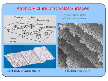
Atomic Picture of Crystal Surfaces
Terraces, steps, kinks, adatoms and vacancies
STM image of Si(001)
STM image of vicinal Si(111)
2
Three Growth Modes
?s gt ?f ?sf With misfit
If ?s gt ?f ?sf
?s lt ?f ?sf
Film
Substrate
Layer-by-layer (Frank-Van der Merwe)
3D islanding (Volmer-Weber)
Layer-by-layer followed by 3D islanding (Stranski
-Krastanov)
?s surface energy of substrate ?f surface
energy of film ?sf interface energy of
substrate-film
3
Stranski-Krastanov growth of Ge on Si(001)
100
pyramids
huts
Wetting layer 2.5 ML Ge, 475 C, (44nm)2
3D islands formation 3.5 ML Ge, 475C, (110nm)2
4
MBE grown GaAs-AlxGa1-xAs superlattice
Bang gap lattice constant for alloy
semiconductors
5
Misfit Dislocations
Threading dislocation
misfit dislocation
6
Molecular Beam Epitaxy (MBE)
7
Real-time monitoring of MBE usingReflection
high-energy electron diffraction (RHEED)
3D growth
RHEED Pattern
Surface reconstruction
Source off
RHEED intensity oscillation
8
Vapor Phase Epitaxy (VPE)
Horizontal reactor
Vertical reactor
Barrel reactor
9
Liquid Phase Epitaxy (LPE)
10
Carrier Mobility Concentration Measurements
Hall Effect
Doping Profile N(x)
I
VH
w
B
x
x
Van der Pauw Test Pattern
Depletion zone
N(x)
Schottky junction
V
C(V) ??0A/x