
The APV Emulator (APVE) - PowerPoint PPT Presentation
1 / 8
Title:
The APV Emulator (APVE)
Description:
The APV Emulator (APVE) What does the APVE do & why ? Task 1. The APV25 has a 10 event buffer in de-convolution mode. Readout of an event = 7 s – PowerPoint PPT presentation
Number of Views:84
Avg rating:3.0/5.0
Title: The APV Emulator (APVE)
1
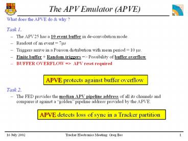
The APV Emulator (APVE)
What does the APVE do why ?
- Task 1.
- The APV25 has a 10 event buffer in de-convolution
mode. - Readout of an event 7?s
- Triggers arrive in a Poisson distribution with
mean period 10 ?s. - Finite buffer Random triggers gt Possibility of
buffer overflow - BUFFER OVERFLOW gt APV reset required
APVE protects against buffer overflow
- Task 2.
- The FED provides the median APV pipeline address
of all its channels and compares it against a
golden pipeline address provided by the APVE.
APVE detects loss of sync in a Tracker partition
2
What does APVE do why ?
- Primary task Preventing buffer overflow in APVs
- Its takes too long to send a buffers full
signal from APVs in the tracker to Trigger
Control System (TCS). - Therefore require an APV close to the TCS.
- Secondary task Synchronisation check
- All APV data frames include the memory cell
(pipeline) address used to store the L1A data in
the APV. - The pipeline address is sent to all FEDs to
ensure that all APVs are in-sync.
Reset and L1A
(min period 75ns)
TCS Inhibit L1A?
Busy
Tracker
APV in deconvolution mode
APVE
1 Full
2 Full
3 Empty
Pipeline address
10 Empty
Data frame
(period 7000ns)
FED Data OK?
3
How does APVE work ?
- L1A Throttle
- A counter keeps track of the number of filled APV
buffers. - L1A gt INCREMENTS counter.
- Output frame gt DECREMENTS the counter.
- Reset gt CLEARS the counter.
- APVE must receive the same L1As and Resets as
APVs within the Tracker or System fails - When the counter reaches preset values it asserts
Warn followed by Busy. - Synchronisation check
- Header on APV data frame provides pipeline address
Reset
L1A
APVE
Real APV25
APV data frame
INCREMENT
Header recognition
CLEAR
Frame output signal
Buffer counter
DECREMENT
Assert busy?
Pipeline address to FEDs
Busy
4
Control structure
- Control Feedback Structure.......
- APVE receives Clk, BC0, L1A, L1Reset from Central
Local TCS - APVE user selects CTCS, LTCS or neither via VME
(i.e. just like TTCci) - APVE sends Warn, Busy, Out-Of-Sync, Ready etc to
Central Local TCS - Sync Check info for FED
- Pipeline address transmitted to FED via TTCci B
channel.
CTCS
LTCS
APVE
TTCci/ex/tx
?
FEC
FMM Fast Merge Module
CCU Ring
Reset L1As
APV
Fast feedback
Pipeline address
?
FED
Data
5
Pipeline address and TTC System
- Pipeline address sent asynchronously via B
channel - Must reach the FED before the FED is ready to
check the pipeline address - Pipeline address must not be blocked by sync B
channel commands for long time period - Solution gt Guaranteed async bandwidth on B
channel of 42clks every 280clks - TCS (Central Local)
- TCS must separate B channel commands by 88 clk
cycles - Tracker TTCci
- Must follow certain rules. All B channel
commands must - be initiated by TCS
- have the same inhibit duration of 42 clock
cycles - have the same inhibit delay (must be non zero if
we require doubles)
Pipeline address transmission started before next
inhibit starts
TCS starting B chan commands/data
BGo_X (1)
BGo_Y (1)
Inhibits
Inhibit_X (42)
Inhibit_X (42)
Sync_Y
Sync_X (16/42)
Pipe Address_B (42)
B Chan Data
6
PCB Design
LEDs
Headers for APV25 daughter card
Switch to display either APVE, FMM or combined
feedback status
All logic in Xilinx 1M gate Virtex2 FPGA
Pipeline address sent to TTCci
Central Local TCS in
Headers for a daughter card that will emulate
TCS for testing
Central Local TCS out
FMM in
7
HDL Design
History.... 1k deep BC (12bit), OC (32bit) and
feedback status (4bit)
VME to Wishbone
APV SIM
APV REAL
APVE (i.e. APV25 buffer status)
I2C interface for real APV25
Merge APVE and FMM
History recorded for........ APVE, FMM, CTCS, LTCS
8
Conclusions
- PCB Design
- Final artwork check
- Manufacture
- PCB
- Assembly
- VHDL Design
- Design
- Modify history to use Dual Port RAM in FPGA
- Minor modifications to other parts
- Synthesis
- Add complex timing requirements to APV_SIM (VHDL
implementation of APV)
- Testing
- Simple TCS emulation in APVE FPGA
- Daughter card to drive LVDS signals from FPGA to
front panel
Recommended
CrystalGraphics Presentations


