
Output stages and power amplifiers
1 / 9
Title: Output stages and power amplifiers
1
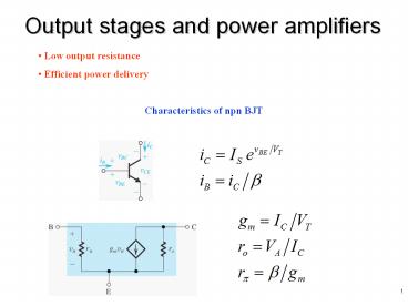
Output stages and power amplifiers
- Low output resistance
- Efficient power delivery
Characteristics of npn BJT
2
Classification of Output Stages
sinusoidal input signal
Figure 14.1 Collector current waveforms for
transistors operating in (a) class A, (b) class
B, and (c) class AB amplifier stages.
3
Class A Output Stage
transfer characteristic
Figure 14.2 An emitter follower (Q1) biased
with a constant current I supplied by transistor
Q2.
4
Signal Waveforms
Figure 14.4 Maximum signal waveforms in the
class A output stage of Fig. 14.2 under the
condition I VCC /RL or, equivalently, RL VCC
/I.
5
Power-Conversion Efficiency
6
Class B Output Stage
transfer characteristic
Figure 14.5 A class B output stage.
7
Power-Conversion Efficiency
8
Power Dissipation
Figure 14.8 Power dissipation of the class B
output stage versus amplitude of the output
sinusoid.
9
Crossover Distortion
Figure 14.7 Illustrating how the dead band in
the class B transfer characteristic results in
crossover distortion.
Recommended
CrystalGraphics Presentations


