1. MBE Growth - PowerPoint PPT Presentation
Title:
1. MBE Growth
Description:
MBE-Grown Nano Wires and Dots ... stacking and anisotropy of these chains leads to polarization dependent photoluminescence at temperatures that allows carrier ... – PowerPoint PPT presentation
Number of Views:109
Avg rating:3.0/5.0
Title: 1. MBE Growth
1
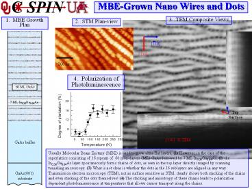
MBE-Grown Nano Wires and Dots
3. TEM Composite Views
1. MBE Growth Plan
2. STM Plan-view
4. Polarization of Photoluminescence
60 ML GaAs
7 ML In0.36Ga0.64As
Usually Molecular Beam Epitaxy (MBE) is used to
grow ultra-flat layers. (1) However, in the case
of the superlattice consisting of 16 repeats of
60 monolayers (ML) GaAs followed by 7 ML
In0.36Ga0.64As, (2) the In0.36Ga0.64As layer
spontaneously forms chains of dots, as seen in
the top layer directly imaged by scanning
tunneling microscopy. (3) What is not clear is
whether the dots in the 16 sublayers are aligned
in any way. Transmission electron microscopy
(TEM), not as surface sensitive as STM, clearly
shows both stacking of the chains and even
stacking of the dots themselves! (4) The stacking
and anisotropy of these chains leads to
polarization dependent photoluminescence at
temperatures that allows carrier transport along
the chains.
2
MBE-Grown Nano Wires and Dots
REU students, Erica Elvey and Byron Williams, at
Arkansas involved with sample transport on
Arkansass multi-chamber Molecular Beam Epitaxy
(MBE) System.
Spreading the word undergraduates and school
teachers are involved in the research in
epitaxial growth at CSPIN. Exposing them to
materials research helps them understand the
basis of modern nanoelectronics.
Oklahoma high school teachers, Jason Rausch and
David Askey, meet with researcher Tetsuya
Mishima, who uses a crystal model to explain the
affect of sample orientation on the Transmission
Electron Microscope (TEM) image.

