OUTLINE - PowerPoint PPT Presentation
1 / 14
Title:
OUTLINE
Description:
Turn-Off Transient In order to turn the diode off, ... 1.1 Silicon Crystal Structure Author: Blyang Last modified by: Tsu-Jae King Created Date: 3/28/2000 4:44:02 PM – PowerPoint PPT presentation
Number of Views:39
Avg rating:3.0/5.0
Title: OUTLINE
1
Lecture 20
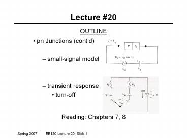
- OUTLINE
- pn Junctions (contd)
- small-signal model
- transient response
- turn-off
- Reading Chapters 7, 8
2
Small-Signal Model of the Diode
Small signal equivalent circuit
i
va
C
R1/G
?
Small-signal conductance
3
Review Charge Storage in pn-Diode
4
- 2 types of capacitance associated with a pn
junction - CJ depletion capacitance
- (due to variation of depletion charge)
- CD diffusion capacitance
- (due to variation of stored minority charge in
the quasi-neutral regions) - For a one-sided pn junction, QP gtgt QN
- so Q QP QN ? QP
5
Depletion Capacitance
What are three ways to reduce Cdep?
6
Total pn-Junction Capacitance
i
va
R1/G
?
- CD dominates at moderate to high forward biases
- Cdep dominates at low forward biases, reverse
biases
7
CJ-vs.-VA (Reverse Bias)
8
Example
If the slope of the (1/Cdep)2 vs. VA
characteristic is -2x10²³ F-2 V-1, the intercept
is 0.84V, and A is 1 mm2, find the lighter and
heavier doping concentrations Nl and Nh.
Solution
9
Summary Small Signal Model
Depletion capacitance
Conductance
Diffusion capacitance
10
Transient Response of pn Diode
- Suppose a pn-diode is forward biased, then
suddenly turned off at time t 0. Because of
CD, the voltage across the pn junction depletion
region cannot be changed instantaneously. - The delay in switching between
- the ON and OFF states is due
- to the time required to change
- the amount of excess minority
- carriers stored in the
- quasi-neutral regions.
11
Turn-Off Transient
- In order to turn the diode off, the excess
minority carriers must be removed by net carrier
flow out of the quasi-neutral regions and/or
recombination - Carrier flow is limited by the switching
circuitry
12
Decay of Stored Charge
- Consider a pn diode (Qp gtgt Qn)
Dpn(x)
i(t)
ts
t
vA(t)
t
For t gt 0
ts
13
Examples (qualitative)
Decrease tp
Increase IF
Increase IR
i(t)
i(t)
i(t)
ts
ts
ts
t
t
t
14
Storage Delay Time ts
- ts is the primary figure of merit used to
characterize the transient response of pn
junction diodes - By separation of variables and integration from t
0 to t ts, noting that - and making the approximation
- We conclude that


![[PDF] DOWNLOAD FREE Clinical Outline of Oral Pathology: Diagnosis and PowerPoint PPT Presentation](https://s3.amazonaws.com/images.powershow.com/10076578.th0.jpg?_=20240711025)


![[READ]⚡PDF✔ Black Letter Outline on Contracts (Black Letter Outlines) 5th Edition PowerPoint PPT Presentation](https://s3.amazonaws.com/images.powershow.com/10044064.th0.jpg?_=20240531080)


