Photodetectors - PowerPoint PPT Presentation
1 / 23
Title:
Photodetectors
Description:
Planar diffusion diode is a basic junction photodiode. A type junction describes a heavily ... Illumination window with an annular electrode for photon passage. ... – PowerPoint PPT presentation
Number of Views:197
Avg rating:3.0/5.0
Title: Photodetectors
1
Photodetectors
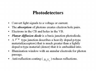
- Convert light signals to a voltage or current.
- The absorption of photons creates electron hole
pairs. - Electrons in the CB and holes in the VB.
- Planar diffusion diode is a basic junction
photodiode. - A type junction describes a heavily doped
p-type material(acceptors) that is much greater
than a lightly doped n-type material (donor) that
it is embedded into. - Illumination window with an annular electrode for
photon passage. - Anti-reflection coating ( ) reduces
reflections.
2
Photodetectors
- The side is on the order of less than a
micron thick (formed by planar diffusion into
n-type epitaxial layer). - A space charge distribution occurs about the
junction within the depletion layer. - The depletion region extends predominantly into
the lightly doped n region ( up to 3 microns max) - Electrodes in the diagram are the external
contacts. - The degree to which photons penetrate through the
layers is dependant upon radiation wavelength.
3
Photodetectors
- Short wavelengths (ex. UV) are absorbed at the
surface. - Longer wavelengths (IR) will penetrate into the
depletion layer. - What would be a fundamental criteria for a
photodiode with a wide spectral response? - A thin p-layer and a thick n layer.
- What does thickness of the depletion layer
determine (along with reverse bias)? - Diode capacitance.
- What does component capacitance dictate to?
- Response time.
4
Photodetectors
- Lower doping levels cause depletion region to
become thicker which in turn reduces diode
capacitance. - PIN photodiode implements this concept by
insertion of a thick, high Z low doped n-type
layer (middle layer) between the p and n layers
of the original model. - The middle layer is called the intrinsic layer or
I-layer. - A moderate quantity of reverse bias can extend
the depletion layer to the bottom of the I-layer. - Result 1. Faster response time.
- 2. Improved (wider) spectral
response.
5
Photodetectors
- Refer to figure 5.1
- Condition
- Assume a reverse bias condition (Vr) applied to
the device. - The depletion layer presents a high resistance
under this condition and a voltage of Vr Vo is
developed across W. (Vo is a built in voltage). - An E field develops in the depletion region and
can be determined by integration of the net space
charge density pnet. - The field is not uniform. It is maximum at the
junction and tapers into the n region.
6
Photodetectors
- Regions outside the depletion region (neutral
regions) hold majority carriers. - These neutral regions can be considered resistive
extensions of electrodes to the depletion region. - Condition
- A photon with an energy greater than bandgap (
) is incident. - Result photon is absorbed and generates
(photogenerates) a free EHP typically in the
depletion layer (electron in CB and hole in VB).
7
Photodetectors
- The E field separates the electron and hole and
causes them to drift in opposite directions until
they reach neutral regions. - The drifting carriers generate a photocurrent in
the external circuit developing an electrical
signal. - The photocurrent exist for a time frame equal to
the time it takes for the electron and hole to
cross the depletion layer (W) and arrive at the
neutral region. - The magnitude of the photocurrent ( ) is
dependant on the number of EHPs generated and the
drift velocities of the carriers while moving
across the depletion layer.
8
Photodetectors
- Note the absorption of photons occurs over a
distance that is dependant on wavelength.
Remembering that the distribution of the field is
not uniform tells us that determining the time
dependence of the photocurrent signal is
difficult. - The resultant photocurrent is a result of
electron flow only not hole migration. - Integrating the hole current to calculate the Q
charge will show that the total photogenerated
electrons is (electrons) and not
(electrons and holes).
9
(No Transcript)
10
(No Transcript)
11
(No Transcript)
12
(No Transcript)
13
(No Transcript)
14
(No Transcript)
15
(No Transcript)
16
(No Transcript)
17
(No Transcript)
18
(No Transcript)
19
(No Transcript)
20
(No Transcript)
21
(No Transcript)
22
(No Transcript)
23
(No Transcript)


