Low Power - PowerPoint PPT Presentation
Title:
Low Power
Description:
... small chronic impants, the power dissipation should not exceed a few hundred ... Power dissipation in the circuit is acceptable, but it is still not close to 1 ... – PowerPoint PPT presentation
Number of Views:60
Avg rating:3.0/5.0
Title: Low Power
1
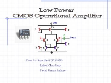
Low Power CMOS Operational Amplifier
Done By Raza Hanif (3336928) Raheel
Choudhary Fawad Usman Rathore
2
Contents of Presentation
- Background and literature review
- Different applications of CMOS OpAmp
- Choice of complex electronic system
- proposed circuit (cmos opamp) to be implemented
in the system -gt In the Book - analysis of proposed circuit
- Improved, and more complex circuit
- Analysis
- System Analysis
- Conclusion
3
BackGround
Complementary Metal-Oxide-Semiconductor (CMOS)
technology is circuit implementation using both
pMOS and nMOS transistors on the same silicon
chip.
CMOS designs typically offer high gain and speed
at low power consumption.
CMOS scales well to smaller devices without
drastic changes in performance.
4
This device is commonly used to amplify small
signals, to add/subtract voltages, and in active
filtering.
It must have high gain, low current draw, and
should function over a variety of frequencies.
5
In Context with Textbook
TTL LOGIC
OP741
6
Why CMOS over TTL?
MOSFETS consume less power in the driver circuit.
MOSFETS have greater bandwidth.
MOSFETS are thermally more stable.
MOSFETS are considerably faster than BJTs.
CMOS ICs use much less power than TTL
7
Analysis of a Complex Electronic System
The input consists of differential electrode
inputs and the outputs are from an amplifier, a
peak detector, a trough detector, and a level
detector.
A trough is a noticeable decline in the
signal strength
8
Implication of CMOS (OTA) amplifier in neural
amplifier
There is a great demand for technologies that
enable neuroscientists and clinicians to observe
the simultaneous activity of large numbers of
neurons in the brain.
While there are microelectronic devices being
developed for small-scale amplification of the
weak bioelectrical signals, existing circuits
typically have unacceptable noise levels or
consume too much power to be fully implanted in
large quantities.
In our electronic system, the bioamplifier must
dissipate little power so that surrounding
tissues are not damaged by heating. A heat flux
of only 80 mW/cm2 can cause necrosis in muscle
tissue.
In small chronic impants, the power dissipation
should not exceed a few hundred miliwatts.
Necrosis accidental death of cells and living
tissue.
9
Main Objective
Design and testing of a fully integrated
amplifier suitable for recording biological
signals from the millihertz range to 7 kHz.
Design such that the amplifier offers the best
power noise tradeoff.
10
Operational Transconductance Amplifier (OTA)
Pg. 885 in textbook
11
Operational Transconductance Amplifier (OTA)
The input voltage controls an output current by
means of the device transconductance, labeled gm.
What is important and useful about the OTAs
transconductance parameter is that it is
controlled by an external current, the amplifier
bias current, IABC , so that one obtains
From this externally controlled transconductance,
the output current as a function of the applied
voltage difference between the two input pins,
labeled v and v-, is given by
12
Analysis of OTA Circuit
Power dissipation in the circuit is acceptable,
but it is still not close to 1 mW, which is ideal
for biosignal amplifiers.
Possible Solutions I) Either, try to improve
this circuit II) Come up with another circuit
that can supply high enough open loop gain, with
low power dissipation.
13
One possible design for a Low power CMOS
Operational Amplifier
14
AC Analysis of the amplifier
DC Gain of this circuit is about 145 dB
15
Power Dissipation of the amplifier
(ID1 ID2 ID3)(VDD-VSS)
The circuit dissipates only about 180 uW of
power, which is quiet low compared to the circuit
analyzed before
16
Result on the Oscilloscope
17
Transient Response of the Circuit
Time domain response of the circuit when it is
excited with a sinusoidal signal.
18
Closed Loop Circuit with Rf Rs in inverting
configuration
19
Result on the Oscilloscope
20
Many other design possibilities
21
Conclusion
The design process that was followed resulted in
a CMOS operational amplifier design that at least
met and, in a few cases, exceeded the design
objectives by a large margin. The notable
performance areas were the DC open loop gain of
145 dB, and the power consumption of 180 uW.
Also, the settling time was quite low as can be
seen by the transient response of the circuit,
which means the circuit is relatively fast.
A great deal was learned in the design process,
including how to approach a design project, the
tradeoffs involved in a CMOS op-amp design,
patience, and how to stay up late.
There could still be a lot improved in this
circuit, but requires knowledge that is beyond
the scope of this course, mainly in the field of
VLSI.
22
References
R. R. Harrison and C. Charles, "A low-power
low-noise CMOS amplifier for neural recording
applications," IEEE J. Solid-State Circuits, vol.
38, pp. 958-965, 2003.
Yiqin Chen, Mark E. Schlarmann and Randall L.
Geiger, "An Improved design Formulation for
design and Optimization of Operational
Amplifiers," MWSCAS99 The 43rd Midwest Symposium
on Circuits and Systems, New Mexico, USA, 8-11
August, 1999.
Electrophysiology, From http//en.wikipedia.org/
wiki/Electrophysiology. Retrieved on November
10th, 2006.


