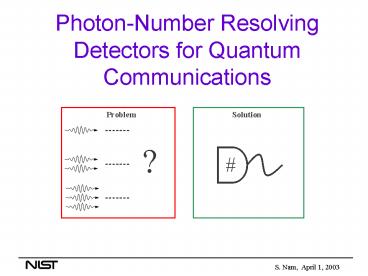
PhotonNumber Resolving Detectors for Quantum Communications
1 / 21
Title:
PhotonNumber Resolving Detectors for Quantum Communications
Description:
Same output signal for varying photon number ... Calorimetric detection of UV/optical/IR photons: ... Constellation-X. SCUBA II: Submillimeter detector array ... –
Number of Views:19
Avg rating:3.0/5.0
Title: PhotonNumber Resolving Detectors for Quantum Communications
1
Photon-Number Resolving Detectors for Quantum
Communications
2
Optical Photon Detectors
- Sae Woo Nam, D. Rosenberg,
- A. J. Miller, A. Salminen,
- E. Grossman, J. M. Martinis
3
Conventional vs. Photon Number Resolving Detectors
4
Transition Edge Sensor (TES) Technology
Energy deposition
Thermometer
Rn
Absorber, C
R
Weak thermal link, g
Thermal sink (50 mK)
T
- Calorimetric detection of UV/optical/IR photons
- Photon(s) absorbed by a heat capacity C
connected to a thermal sink by a weak thermal
link g. - Temperature of the absorber is monitored by an
ultra-sensitive thermometer (superconducting-to-no
rmal transition). - Temperatures are 100 mK to ensure low noise and
high sensitivity. - Our absorber and thermometer are the same
5
Historical Note
- CDMS direct detection of dark matter
- X-ray microanalysis
- Constellation-X
- SCUBA II Submillimeter detector array
- Optical Spectrophotometer with timestamping
6
TES Readout
Output signal is proportional to number of
absorbed photons
- Device is voltage biased
- Current through device is pre-amplified using a
cryogenic SQUID array amplifier - Signal can then be processed using RT electronics
- Optimized now for photon-number resolution, not
speed (trise100 ns, tfall10 ms) - Absorption events show good distinguishability
- Much slower than APDs
7
Devices and Optical Coupling
W TES
Si
25 µm
Al wiring
- TES is 35 nm thick tungsten film, Tc100 mK
- Wiring is 80 nm thick superconducting Al
- Central pixel is 25 µm 25 µm
- Optical photolithographic process
- Optical fiber is 9 µm core SM fiber
- Coupling is lens-free, expect low-loss
- Losses are dominated by reflection and
inefficient optical alignment - Target efficiency gt80 at 1550 nm
8
(No Transcript)
9
- Cryostat
- Commercially available
- Portable (70 kg)
- All electronic cooling
- LN2 fill every 24 hrs.
- LHe fill every 3 days
- Base Tlt100mK for 24 hrs.
- 1.5 hour regeneration time
- Next version, Cryogen Free!
10
1310 nm Weak Coherent Source
PNR
SM Fiber
Pulsed Laser
65 dB
Fiber attenuator
1310 nm or 1550 nm 100 ns wide pulses
11
1550 nm Weak Coherent Source
l1.550 mm
Pulse Height a.u.
12
BU Quantum Optical Setup
Doubles
Coincident
PNR 1
CW Laser
Dichroic
351 nm
BBO
Doubles
PNR 2
3 nm IF
l/2
PBS
Delay
Coincident Rate
Zero Delay
Counts/sec
Delay time
13
LANL Fiber QKD
- Phase encoding
- 1310 nm link
- 1550 nm bright pulse for timing
- Timing / Optical switches
- GPS link for timing
- Stray light
14
Unique Features of TES detectors
- Photon Number Resolution
- Low Noise
- NEP lt 10-19 W/vHz (limited by stray light)
- No Dark Counts
- High QE at telecommunication wavelengths
- 40 intrinsic, gt20 end-to-end measured
- AR coatings give no limit, in principle
- Target of gt80 w/ single layer at 1550 nm
- Crude Spectrometer
- Slow trise100 ns, tfall10 ms
- Cryogenic
15
Work In Progress
- Improving the Quantum Efficiency
- Anti-reflection coatings
- Materials compatibility work
- Speed (MHz)
- Improvements to existing materials, new materials
- New biasing technique
- Putting together systems for broader use
16
Superconducting Fabrication Facility
- 2700 sq ft class 100 space
- I-line 5x lithography
- E-beam lithography
- Reticle generation
- Sputter deposition (x2)
- ECR PECVD deposition
- LPCVD (x2)
- Thermal oxide / diffusion (x2)
- Thermal deposition (x2)
- RIE (x2)
- Plasma etching
- Ion mill etching
- 3 inch wafers
17
Improving the Quantum Efficiency
- Optical coatings
- Thin film dielectrics
- Detector material compatibility
- Tungsten deposition
- Optical characterization and simulation tools
- Spectrophotometer
18
Path to Moores Law
- Combination of electrical circuit, thermal
circuit, and noise sources - More Power speed
- but lower discrimination
- New materials with higher conductance
- Modulate electrical bias
19
System Assembling
- Cryogen based system
- Major parts arriving soon
- No longer borrowing equipment
- Cryogen free system for NIST DARPA QuIST testbed
and Boulder Labs - Cryogenic platform for other detector technologies
20
Next Experiments / Systems
- Source Characterizations
- Weak coherent at 1550nm
- SPDC on demand, NIST Physics Lab
- SPT (now available at NIST EEEL)
- Quantum Optics, BU
- QKD experiments, LANL
- Demonstration of multi-channel system
- Detector loophole free tests of Bells inequality
- Full Bell-State analyzer
21
Conclusion
- Demonstration of first true photon-counting
detector at telecomm wavelengths for quantum
information science and applications - Verification of the Poisson nature of a weak
coherent source - Demonstration of the only telecommunications-wavel
ength system with zero dark counts - Prospects are good for improving QE to gt80 at
1550nm - Truly unique among telecommunication-wavelength
instruments - Ideal for a NIST metrological tool


