Nanoscale Patterning Center Paul R' Berger1,2,3 - PowerPoint PPT Presentation
1 / 1
Title:
Nanoscale Patterning Center Paul R' Berger1,2,3
Description:
EBPG-5000 EBL system provides high resolution, greater accuracy and versatility ... using high-resolution HSQ (hydrogen silsesquioxane) resist ... – PowerPoint PPT presentation
Number of Views:40
Avg rating:3.0/5.0
Title: Nanoscale Patterning Center Paul R' Berger1,2,3
1
Nanoscale Patterning Center Paul R.
Berger1,2,3 1Department of Electrical and
Computer Engineering 2Department of Physics
3Director of Ohios Nanoscale Patterning
Consortium The Ohio State University, Columbus,
OH 43210
ECE Cleanroom Renovations
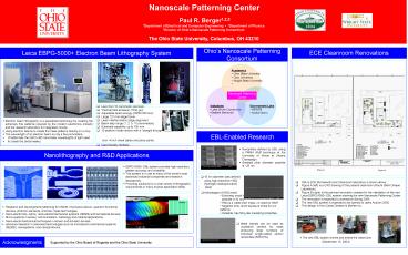
Leica EBPG-5000 Electron Beam Lithography System
Ohios Nanoscale Patterning Consortium
- Academics
- Ohio State University
- Ohio University
- Wright State University
Nanoscale Patterning Center
- Industries
- Lake Shore Cryotronics
- Battelle Memorial
- Government Labs
- WPAFB
- NASA Glenn
- Less than 10 nanometer spot size
- Thermal field emission (TFE) gun
- Adjustable beam energy (20/50/100 KeV)
- Large 127 mm stage travel
- Laser interferometric stage alignment
- Beam step range (1, 2, 5, 10 nanometers)
- Substrate capability up to 150 mm
- 10 position holder airlock with a "straight
through" loading facility - (incl. 4-inch mask plates and piece parts)
- User-friendly interface
- Electron beam lithography is a specialized
technique for creating the extremely fine
patterns required by the modern electronics
industry and the research laboratory for
integrated circuits. - Using electron beams to create the mask patterns
directly on a chip. - The wavelength of an electron beam is only a few
picometers. - (Traditionally the 248 to 365 nanometer
wavelengths of light used - to create the photomasks.)
EBL-Enabled Research
- Nanopillars defined by EBL using a PMMA liftoff
technique at the University of Illinois at Urbana
Champaign - Smallest pillar diameter possible is 25 nm
Nanolithography and RD Applications
- EBPG-5000 EBL system provides high resolution,
greater accuracy and versatility - This system is in use at many of the worlds most
advanced industrial companies and research
laboratories. - Providing solutions for a wide variety of
lithographic requirements in many diverse
application fields.
(Figure A)
(Figure B)
- 15 nm diameter dots defined
- using high-resolution HSQ
- (hydrogen silsesquioxane)
- resist
- OSUs ECE Microelectronics Cleanroom laboratory
is shown above. - Figure A (left) is a CAD drawing of the present
cleanroom (Room 095H Dreese - Laboratory).
- Figure B (right) is the planned renovation
needed for the installation of the new - Leica EBPG-5000 EBL system showing the
new Nanoscale Patterning Center. - The renovation is expected to commence Spring
2005. - The new EBL system is expected to be opened to
users Autumn 2005. - This design is from Camp Dresser McKee Inc.
- Advantages of HSQ resist
- Extremely small features
- possible (lt10 nm)
- HSQ is a viable etch mask- no need for liftoff
- Negative tone- short exposure times for our
patterns - Versatile- has SiO2-like insulating properties
- Research and Development patterning for CMOS,
microwave device, quantum functional devices,
photonic elements, and NGL mask technologies. - Nano-electronics, optics, nano-electromechanical
systems (NEMS) and biomedical devices - Micro-systems in sensor, communication, metrology
and medical applications. - Nano-electromechanical techniques in sensor and
actuator devices. - advanced research in advanced technologies such
as microelectro-mechanical systems (MEMS),
nanosystems, and nanophotonics.
- Metal islands can be used as nucleation centers
for mass producing large numbers of individual
single-walled carbon nanotubes (SWCNTs).
- The new EBL system arrives and enters the
cleanroom - (September 15, 2004)
Acknowledgments
Supported by the Ohio Board of Regents and the
Ohio State University.

