Full Solar Spectrum Photovoltaic MaterialInGaN - PowerPoint PPT Presentation
1 / 5
Title:
Full Solar Spectrum Photovoltaic MaterialInGaN
Description:
Fabrication process could ... low gap cell (InN n/p junction, Eg=0.7 eV) high gap cell (In0.34Ga0.66N n/p ... for high efficiencies in one material system ... – PowerPoint PPT presentation
Number of Views:38
Avg rating:3.0/5.0
Title: Full Solar Spectrum Photovoltaic MaterialInGaN
1
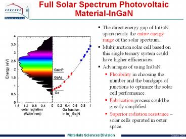
Full Solar Spectrum Photovoltaic Material-InGaN
- The direct energy gap of InGaN spans nearly the
entire energy range of the solar spectrum. - Multijunction solar cell based on this single
ternary system could have higher efficiencies. - Advantages of using InGaN
- Flexibility in choosing the number and the
bandgaps of junctions to optimize the solar cell
performance. - Fabrication process could be greatly simplified
- Superior radiation resistance solar cells
operated in outer space.
2
Progress and Outstanding Issues
- InN
- Energy gap 0.64 to 0.67 eV _at_ RT
- Mobility electrons (2200 to 4000 cm2/Vs), holes
(40 cm2/Vs) - Minority carriers (holes) lifetime (gt 1 to 2 ns)
diffusion length ( 1mm) - Doping n-type (3x10¹⁷ to 1021 cm-3), p-type (mid
1019 cm-3 ?) - Surface electron accumulation (2x10¹³ to 4x10¹³
cm-2) - InGaN (or
InAlN) - Band gap bowing InGaN (1.4 to 1.8 eV), InAlN
(2.7 to 5.5 eV) - Small Stokes shift
- Doping n-type should be easier than p-type
- Composition modulation effects
- Surface electron accumulation in In-rich alloys
(xGalt0.66) - Charge control at heterointerfaces
3
Solutions??
- No charge accumulation at heterointerfaces
- - low gap cell (InN n/p junction, Eg0.7 eV)
high gap cell (In0.34Ga0.66N n/p junction,
Eg2.2 eV) - Compositionally graded n/p junction from xGa0 to
0.66 - Heterointerfaces with large work function p-type
semiconductors (e.g. CuInS2) - Elimination of the accumulation layer through
surface treatments
4
Point-Counter Point
- Advantages
- Massive span in PV energies for high efficiencies
in one material system - Nitrides generally offer recombination
insensitivity to dislocations - Strong band bending is perfect for low surface
recombination velocity
- Disadvantages
- Massive span in PV energies is not in a lattice
matched system - High dislocation density
. - Strong band bending has resulted in inability to
form a solid state junction - P-type doping undemonstrated
- Tunnel junctions probably not possible
- P-type base is usually preferred due to higher
mobility of minority electrons - 3-junction high concentration solar cells are
already in excess of 37.2 efficient
(GaInP/GaAs/Ge Spectrolabs King et al)
5
Low-energy optical transitions
plateau
transition near 1.3 1.4 eV
onset (Eg 0.7 eV)
F. Bechstedt et al., phys. stat. sol. (a) 195,
628 (2003)


