
Controller Implementation--Part I - PowerPoint PPT Presentation
1 / 34
Title:
Controller Implementation--Part I
Description:
NASTY HACK: delay LD through. negative edge triggered FF to. ensure that it won't change during ... Change in response to input changes, independent of clock ... – PowerPoint PPT presentation
Number of Views:41
Avg rating:3.0/5.0
Title: Controller Implementation--Part I
1
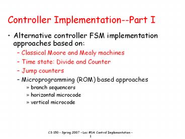
Controller Implementation--Part I
- Alternative controller FSM implementation
approaches based on - Classical Moore and Mealy machines
- Time state Divide and Counter
- Jump counters
- Microprogramming (ROM) based approaches
- branch sequencers
- horizontal microcode
- vertical microcode
2
Cascading Edge-triggered Flip-Flops
- Shift register
- New value goes into first stage
- While previous value of first stage goes into
second stage - Consider setup/hold/propagation delays (prop must
be gt hold)
100
IN Q0 Q1 CLK
3
Cascading Edge-triggered Flip-Flops
- Shift register
- New value goes into first stage
- While previous value of first stage goes into
second stage - Consider setup/hold/propagation delays (prop must
be gt hold)
Clk1
Delay
100
IN Q0 Q1 CLK
4
Clock Skew
- The problem
- Correct behavior assumes next state of all
storage elementsdetermined by all storage
elements at the same time - Difficult in high-performance systems because
time for clock to arrive at flip-flop is
comparable to delays through logic (and will soon
become greater than logic delay) - Effect of skew on cascaded flip-flops
100
In Q0 Q1 CLK CLK1
CLK1 is a delayed version of CLK
original state IN 0, Q0 1, Q1 1 due to
skew, next state becomes Q0 0, Q1 0, and not
Q0 0, Q1 1
5
Why Gating of Clocks is Bad!
gatedClK
BAD
GOOD
Do NOT Mess With Clock Signals!
6
Why Gating of Clocks is Bad!
Do NOT Mess With Clock Signals!
7
Why Gating of Clocks is Bad!
Reset
Reg
Counter
slowClK
Clk
BAD
Do NOT Mess With Clock Signals!
8
Why Gating of Clocks is Bad!
Reset
LD
Reg
Counter
Clk
Better!
Do NOT Mess With Clock Signals!
9
Alternative Ways to Implement Processor FSMs
- "Random Logic" based on Moore and Mealy Design
- Classical Finite State Machine Design
- Divide and Conquer Approach Time-State Method
- Partition FSM into multiple communicating FSMs
- Exploit Logic Block Functionality Jump Counters
- Counters, Multiplexers, Decoders
- Microprogramming ROM-based methods
- Direct encoding of next states and outputs
10
Random Logic
- Perhaps poor choice of terms for "classical" FSMs
- Contrast with structured logic PLA, FPGA,
ROM-based (latter used in microprogrammed
controllers) - Could just as easily construct Moore and Mealy
machines with these components
11
Moore MachineState Diagram
Reset
RES
0
PC
IF0
PC
MAR, PC 1
PC
IF1
Note capture of MBR in these states
Wait/
IF2
Wait/
IF3
MBR
IR
Wait/
OD
11
00
01
10
IR
MAR,
ST0
LD0
AD0
IR
MAR
IR
MAR
BR0
AC
MBR
0
1
Wait/
Wait/
Wait/
BR1
ST1
AD1
LD1
IR
PC
AD2
LD2
MBR
AC
MBR AC
AC
12
Memory-Register Interface Timing
Valid data latched on IF2 to IF3
transition because data must be valid before
Wait can go low
13
Moore Machine Diagram
16 states, 4 bit state register Next State
Logic 9 Inputs, 4 Outputs Output Logic 4
Inputs, 18 Outputs
These can be implemented via ROM or PAL/PLA
Next State 512 x 4 bit ROM Output 16 x 18 bit
ROM
14
Moore Machine State Table
- Reset Wait IRlt15gt IRlt14gt AClt15gt Current
State Next State Register Transfer Ops - 1 X X X X X RES (0000)
- 0 X X X X RES (0000) IF0 (0001) 0 ??PC
- 0 X X X X IF0 (0001) IF1 (0001) PC ? MAR, PC 1
? PC - 0 0 X X X IF1 (0010) IF1 (0010)
- 0 1 X X X IF1 (0010) IF2 (0011)
- 0 1 X X X IF2 (0011) IF2 (0011) MAR ? Mem, Read,
- 0 0 X X X IF2 (0011) IF3 (0100) Request, Mem ?
MBR - 0 0 X X X IF3 (0100) IF3 (0100) MBR ? IR
- 0 1 X X X IF3 (0100) OD (0101)
- 0 X 0 0 X OD (0101) LD0 (0110)
- 0 X 0 1 X OD (0101) ST0 (1001)
- 0 X 1 0 X OD (0101) AD0 (1011)
- 0 X 1 1 X OD (0101) BR0 (1110)
15
Moore Machine State Table
- Reset Wait IRlt15gt IRlt14gt AClt15gt Current
State Next State Register Transfer Ops - 0 X X X X LD0 (0110) LD1 (0111) IR ? MAR
- 0 1 X X X LD1 (0111) LD1 (0111) MAR ? Mem, Read,
- 0 0 X X X LD1 (0111) LD2 (1000) Request, Mem ?
MBR - 0 X X X X LD2 (1000) IF0 (0001) MBR ? AC
- 0 X X X X ST0 (1001) ST1 (1010) IR ? MAR, AC ?
MBR - 0 1 X X X ST1 (1010) ST1 (1010) MAR ? Mem,
Write, - 0 0 X X X ST1 (1010) IF0 (0001) Request, MBR ?
Mem - 0 X X X X AD0 (1011) AD1 (1100) IR ? MAR
- 0 1 X X X AD1 (1100) AD1 (1100) MAR ? Mem, Read,
- 0 0 X X X AD1 (1100) AD2 (1101) Request, Mem ?
MBR - 0 X X X X AD2 (1101) IF0 (0001) MBR AC ? AC
- 0 X X X 0 BR0 (1110) IF0 (0001)
- 0 X X X 1 BR0 (1110) BR1 (1111)
- 0 X X X X BR1 (1111) IF0 (0001) IR ? PC
16
Moore Machine State Transition Table
- Observations
- Extensive use of Don't Cares
- Inputs used only in a small number of statee.g.,
AClt15gt examined only in BR0 state IRlt1514gt
examined only in OD state - Some outputs always asserted in a group
- ROM-based implementations cannot take advantage
of don't cares - However, ROM-based implementation can skip state
assignment step
17
Synchronous Mealy Machines
- Standard Mealy Machine has asynchronous outputs
- Change in response to input changes, independent
of clock - Revise Mealy Machine design so outputs change
only on clock edges - One approach non-overlapping clocks
Synchronizer Circuitry at Inputs and Outputs
18
Synchronous Mealy Machines
Case I Synchronizers at Inputs and Outputs
A asserted in Cycle 0, ƒ becomes asserted after 2
cycle delay! This is clearly overkill!
19
Synchronous Mealy Machine
Case II Synchronizers on Inputs
A asserted in Cycle 0, ƒ follows in next
cycle Same as using delayed signal (A') in Cycle
1!
20
Synchronous Mealy Machines
Case III Synchronized Outputs
A asserted during Cycle 0, ƒ' asserted in next
cycle Effect of ƒ delayed one cycle
21
Synchronous Mealy Machines
- Implications for Processor FSM Already Derived
- Consider inputs Reset, Wait, IRlt1514gt, AClt15gt
- Latter two already come from registers, and are
sync'd to clock - Possible to load IR with new instruction in one
state perform multiway branch on opcode in next
state - Best solution for Reset and Wait synchronized
inputs - Place D flipflops between these external signals
and the - control inputs to the processor FSM
- Sync'd versions of Reset and Wait delayed by one
clock cycle
22
Time State Divide and Conquer
- Overview
- Classical Approach Monolithic Implementations
- Alternative "Divide Conquer" Approach
- Decompose FSM into several simpler communicating
FSMs - Time state FSM (e.g., IFetch, Decode, Execute)
- Instruction state FSM (e.g., LD, ST, ADD, BRN)
- Condition state FSM (e.g., AC lt 0, AC ¹ 0)
23
Time State (Divide Conquer)
T0
Time State FSM
Most instructions follow same basic
sequence Differ only in detailed execution
sequence Time State FSM can be parameterized by
opcode and AC states
T1
Wait/
T2
Wait/
T3
Wait/
T4
Instruction State stored in IRlt1514gt
BRN AC
Recommended
CrystalGraphics Presentations


