
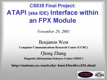
CS535 Final Project: ATAPI aka IDE Interface within an FPX Module
1 / 18
Title:
CS535 Final Project: ATAPI aka IDE Interface within an FPX Module
Description:
Maggie Zhang: VHDL Coding of ATAPI state machine, SDRAM FIFO, ATM encapsulation of ATAPI data. ... data burst ( 2MB) and store it in ATM cells in the SDRAM FIFO. ... –
Number of Views:40
Avg rating:3.0/5.0
Title: CS535 Final Project: ATAPI aka IDE Interface within an FPX Module
1
CS535 Final ProjectATAPI (aka IDE) Interface
within an FPX Module
- November 28, 2001
- Benjamin West
- Computer Communications Research Center (CCRC)
- Qiong Zhang
- Magnetic Information Sciences Center (MISC)
- http//students.cec.wustl.edu/bmw3/hwdb/cs535.sht
ml
2
Project Objectives
- To snoop traffic that traverses ATAPI bus,
capturing contents of data packets. - To observe max throughput achievable on ATAPI
bus, independent of speed at which host can
digest bus transactions. - To apply various of text stream processing (i.e.
matching) on data extracted from ATAPI pkts.
3
Delegation
- Maggie Zhang VHDL Coding of ATAPI state machine,
SDRAM FIFO, ATM encapsulation of ATAPI data. - Ben West Hardware Daughterboard, VHDL coding of
ATM_out State Machine, Electrical Signal
Integrity Verification.
4
ATAPI on FPX Module
Host ATAPI Controller
FPX
RAD
NID
Loopback module
ATAPI bus
ATAPI_to_ATM module
RAD test pins
Hard drive
5
ATAPI on FPX Module
Host ATAPI Controller
FPX
RAD
NID
Loopback module
ATAPI bus
ATAPI_to_ATM module
RAD test pins
Hard drive
6
Pacer Module (from MP5)
Out to NID
From NID
7
Pacer Modulemodified to accept data from ATAPI
bus
From RADTest
Out to NID
8
ATAPI_to_ATM Module (up close, conceptual)
SDRAM- based FIFO
Data extracted from ATAPI pkts
ATAPI bus
Extracted data
ATAPI FSM
ATM_out FSM
Assemble into ATM cells
CTRL cell
RAD CLK
9
ATAPI_to_ATM Module (up close)
SDRAM
SDRAM Controller
ATAPI_to_ATM module
ATAPI FSM
Clk_en_word_rad
CellFifo
Data_in
WriteRequest
Soc_out
ReadRequest
Data_from_IDE
16
WriteGrant
Control
Tca_in
ReadGrantt
64
WriteData
Data_out
ReadeData
64
64
32
Get Cell
Push Cell
Pull Cell
Send Cell
10
ATAPI FSM (see figs at end of presentation for
reference)
IDLE
Termination
Termination
DMARQ1 DMACK1 STOP0 HDMARDY1
Termination
Termination
InitialDMA
DSTROBE edge/ Set enable signal
DSTROBE edge/ Set enable signal
IDE_1
IDE_3
DSTROBE edge/ Set enable signal
DSTROBE edge/ Set enable signal
IDE_2
11
Also a Hardware Component
- Daughterboard required to convert 5V ATAPI bus to
3.3V for RAD. - Must provide external termination to RAD test
pins to preserve signal integrity.
12
Status
- VHDL
- Done with coding, need simulation.
- Currently using RAD clock to sample all ATAPI
signal, OK with Ultra DMA mode 0 (8 MHz), may
need Asynchronous circuit for higher mode Ultra
DMA - Send control signal from NID to initialize ATAPI
FSM - HARDWARE
- Daughterboard designed and etched, to be
soldered. - Electrical Termination needs to be verified on
O-scope.
13
Working Prototype (by beginning Dec.)
- Can snoop ATAPI traffic in UDMA mode 0 (120ns
cycle time) - Can capture an entire data burst (lt2MB) and store
it in ATM cells in the SDRAM FIFO.
14
ATAPI Protocol ReferenceInitiating UDMA Mode 0
Data Bursthttp//www.t13.org
15
ATAPI Protocol ReferenceSustained UDMA Mode 0
Data Bursthttp//www.t13.org
16
ATAPI Protocol ReferenceHost Pausing UDMA Mode 0
Data Bursthttp//www.t13.org
17
ATAPI Protocol ReferenceDevice Terminating UDMA
Mode 0 Data Bursthttp//www.t13.org
18
ATAPI Protocol ReferenceHost Terminating UDMA
Mode 0 Data Bursthttp//www.t13.org