Process Flow Direction
1 / 2
Title:
Process Flow Direction
Description:
... no waste material and therefore the board utilises the least possible laminate. ... manufacturing panel as supplied by the laminate provider to the PCB producer. ... –
Number of Views:24
Avg rating:3.0/5.0
Title: Process Flow Direction
1
Optimised Panelisation Waste Material Most
PCBs with surface mount technology or
conventional through-hole components require
peripheral waste strip for the purpose of
mechanical handling, conveying and clearance for
edge connectors etc. However, although waste
strip does not constitute any active part of the
working circuitry, it does contribute towards
material consumption and therefore adds to the
board price. Many Sub-contract assembly houses
default to a standard assembly panel
approximately A4 in size with a 10mm wide waste
strip that runs around the periphery of the
circuit, yet this is not always necessary. As
the panel generally moves through the assembly
process in only one plane only, it is often
acceptable to utilise a waste strip that runs
down both sides of the board with no waste strip
on either the leading or trailing edge. The
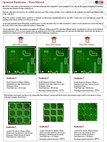
example below shows the material consumption of a
200mm x 200mm square PCB with three different
options of panelisation, with an overall
optimised material reduction of 15. As base
material alone can represent up to 23 of the
manufacturing cost (and more for high layer count
work), this equates to a potential price
reduction of 3.5 on the buy price of the PCB
without any compromise.
Process Flow Direction
Process Flow Direction
Process Flow Direction
Panelisation 1 Board dimension 200mm x
200mm Peripheral waste strip 10mm all sides Route
gap 2.4mm Total Panel size 505.35 mm2
Panelisation 2 Board dimension 200mm x
200mm Peripheral waste strip 10mm on 2x
sides Route gap 2.4mm Total Panel size 449.60
mm2 Percentage material reduction 11
Panelisation 3 Board dimension 200mm x
200mm Peripheral waste strip 5mm on 2x
sides Route gap 2.4mm Total Panel size 429.60
mm2 Percentage material reduction 15
With multiple circuit panels and the use of
scoring rather than routing to separate
individual circuits, the potential savings could
be even greater as shown in the three examples
shown below
Panelisation 2 1 panel of 9x circuits, 40mm x
40mm 5mm waste strip around 2x sides gaps Route
gap 2.4mm between all circuits Total Panel size
215.54mm2 Percentage material reduction 29
Panelisation 3 1 panel of 9x circuits, 40mm x
40mm 5mm waste strip around 2x sides Score lines
between all circuits Total Panel size
156.00mm2 Percentage material reduction 49
Panelisation 1 1 panel of 9x circuits, 40mm x
40mm 10mm waste strip around 4x sides
gaps Route gap 2.4mm between all circuits Total
Panel size 304.15 mm2
2
- Optimised Panelisation Best Fit Scenario
- The most cost effective way to buy a board with
regards to material consumption from a customer
perspective would be single circuits that are not
panelised. - The reasons for this are two-fold. Firstly there
is no waste material and therefore the board
utilises the least possible laminate. Secondly,
it allows the PCB manufacture to best fit the
individual circuits within the much larger
manufacturing panel. - Unfortunately, with the use of surface mount (SM)
technology, it is generally necessary to place
waste strips even on single circuits to
facilitate auto-population of components to give
a holding area and create a clearance for the
pick-and-place system towards the edge of the
board. - A fairly typical manufacturing panel for assembly
purposes would be A4 (210mm x 300mm), but this
panel itself would be routed out of a much larger
manufacturing panel as supplied by the laminate
provider to the PCB producer. - It is an important function of the manufacturing
planning and quotation functions to make optimum
use of the manufacturing panels with the least
waste possible, as this waste is generally costed
into the job. - For this reason, it is sometimes possible to
produce three different quotations for a PCB - Option A Best fit for the end customer (little
or no waste strip) - Option B Best fit for the assembly line or
contractor (enough waste strip to convey and grip
the boards) - Option C Best fit for the PCB manufacturer (a
panel layout that efficiently fits in to the
manufacturing panel)
- Option B PCB Panelised to Assembly best fit.
2x Panels each consisting of 9x circuits with
poor yield from the manufacturing panel resulting
in significant waste.
- Option C PCB Panelised to Assembly best fit.
6x Panels each consisting of 6x circuits with
efficient yield from the manufacturing panel
resulting in negligible waste.


