SLAAC Technology - PowerPoint PPT Presentation
1 / 19
Title:
SLAAC Technology
Description:
Distributed ACS architecture for research lab and ... Myricom LANai. Future PPC Connector. Myricom 8-port Switch. SAN connector. VME Myrinet P0 connector ... – PowerPoint PPT presentation
Number of Views:51
Avg rating:3.0/5.0
Title: SLAAC Technology
1
SLAAC Technology
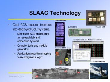
Tower of Power
- Goal ACS research insertion into deployed DoD
systems. - Distributed ACS architecture for research lab and
embedded systems. - Compiler tools and module generators.
- Application/algorithm mapping to reconfigurable
logic .
SLAAC2 VME
SLAAC1 PCI
Compiler tools and Module Generators
Annotated SAR Image
Annotated IR/ATR Image
2
SLAAC Affiliates
3
Application Challenges
- SLAAC applications have a variety of physical
form factors and scalability requirements. - However, most development will occur in
university labs.
NVL IR/ATR
Sandia SAR/ATR
NUWC Sonar Beamforming
4
SLAAC Approach
- SLAAC defines a scalable, portable, distributed
systems architecture based on a high speed
network of ACS accelerated nodes.
- SLAAC has created
- Family of ACS accelerators in multiple form
factors. - ACS system level API and runtime environment.
- ACS design/debugging tools.
5
Programming Model
- ACS API defines a system of nodes and channels.
- System dynamically allocated at runtime.
- Channels stream data between FIFOs on host/nodes.
- API provides common control primitives to a
distributed system. - configure, readback, set_clock, run, etc.
Hosts
Nodes
Network
6
VT Tower of Power
- Completed implementation of v1.0 of API.
- Implemented in C (callable from C).
- Software NT MPI (WMPI MPI-FM).
- Hardware WildForce, SLAAC-1 PCI.
- Runs on the Tower of Power.
- 16-node cluster of PCs.
- WildForce board on each PC.
- Myrinet network connecting all PCs.
7
FPGA Structure
- Mesh of programmable logic blocks with a
programmable interconnect.
Source Xilinx XC4000 Data Book
8
Source Xilinx XC4000 Data Book.
9
Interconnection Network
- Mesh has interconnections of different lengths.
Source Xilinx XC4000 Data Book
10
SLAAC1 PCI Architecture
- Full-sized 64-bit PCI card.
- One XC4085 and two Xilinx XC40150s (750K user
gates). - Twelve 256Kx18 ZBT SSRAM memories (gt5MB user
memory). - External I/O connectors.
- Xilinx 4062 PCI interface.
- Two 72-bit FIFO ports.
- External memory bus.
- 100MHz programmable clock.
72/
72 /
11
SLAAC1 Front
Memory Module (3)
SLAAC-1 PCI
12
SLAAC2 Architecture
- Two independent SLAAC1 boards in single 6U VME
mezzanine. - Four XC40150s, two XC4085s - 1.5M gates total.
- Twenty 256Kx18 SSRAMs.
- Sacrificed external memory bus.
40 /
40 /
72/
72/
13
CSPI Baseboard
PPC 603
Myricom LANai
Future PPC Connector
SAN connector
Myricom 8-port Switch
VME Myrinet P0 connector
14
SLAAC2 Front
15
SLAAC-1V Architecture
- Three Virtex 1000.
- 3M logic gates _at_ 200MHz.
- Use Xilinx 64/66 core.
- Virtex100 configuration controller, FLASH,
SRAM. - Ten 256Kx36 ZBT SRAMs.
- Bus switches allow single-cycle memory bank
exchange between X0 and X1/X2. - Three I/O connectors.
- Three port crossbar gives access to other FPGAs
or local external I/O connector.
X1
X2
72
60
X
X
X
72
X0
IF
X0
72
72
User
Interface
CC
F
S
64/66 PCI
16
SLAAC-1V
17
SV2 Block Diagram
- (8) 512Kx36 200MHz ZBT SRAM.
- X0 is Virtex-II 6000 (6M Gates, 824 User IO).
- (2) 144-pin SO DIMM (512MB PC100 SDRAM).
- IF is Virtex-II 1000 FPGA with 64/66 PCI.
- (2) 72-pin LVTTL or (4) 16-pair LVDS busses.
- Processor PMC I/O Connectors (set of 5) (about
160 pins).
6
1
2
X0 XC2V6000
SODIMM
SODIMM
IF XC2V1000
3
5
4
18
SV2 Placement
- Front Side
- IF FPGA.
- X0 FPGA.
- PMC Connector Set (5)
- Tall power supply on far end of board.
- Limit component height under PMC to specs!
- Back Side
- (8) ZBT SRAM near X0.
- (2) SO DIMM or discrete SDRAM chips near IF.
- Limit component heights to PCI specs!
Power Supply
PrPMC
X0
IF
19
Example Processor PMC
- See the draft athttp//www.mcg.mot.com

